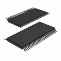
74ALVC16835ADGG:11 NXP Semiconductors, 74ALVC16835ADGG:11 Datasheet - Page 2

74ALVC16835ADGG:11
Manufacturer Part Number
74ALVC16835ADGG:11
Description
74ALVC16835ADGG/TSSOP56/REEL13
Manufacturer
NXP Semiconductors
Series
74ALVCr
Datasheet
1.74ALVC16835ADGG11.pdf
(12 pages)
Specifications of 74ALVC16835ADGG:11
Logic Type
Buffer/Line Driver, Non-Inverting
Number Of Elements
1
Number Of Bits Per Element
18
Current - Output High, Low
24mA, 24mA
Voltage - Supply
2.3 V ~ 3.6 V
Operating Temperature
-40°C ~ 85°C
Mounting Type
Surface Mount
Package / Case
56-TSSOP
Lead Free Status / RoHS Status
Lead free / RoHS Compliant
Other names
74ALVC16835ADG-T
74ALVC16835ADG-T
935267333118
74ALVC16835ADG-T
935267333118
1. C
Philips Semiconductors
FEATURES
DESCRIPTION
The 74ALVC16835A is a 18–bit registered driver. Data flow is
controlled by active low output enable (OE), active low latch enable
(LE) and clock inputs (CP).
When LE is LOW, the A to Y data flow is transparent. When LE is
HIGH and CP is held at LOW or HIGH, the data is latched; on the
LOW to HIGH transient of CP the A-data is stored in the
latch/flip-flop.
When OE is LOW the outputs are active. When OE is HIGH, the
outputs go to the high impedance OFF–state. Operation of the OE
input does not affect the state of the latch/flip-flop.
To ensure the high-impedance state during power up or power
down, OE should be tied to V
minimum value of the resistor is determined by the current-sinking
capability of the driver.
QUICK REFERENCE DATA
GND = 0 V; T
NOTES:
2000 Mar 14
Wide supply voltage range of 1.2 V to 3.6 V
Complies with JEDEC standard no. 8-1A.
CMOS low power consumption
Direct interface with TTL levels
Current drive
MULTIBYTE
Low inductance multiple V
and ground bounce
Output drive capability 50
Input diodes to accommodate strong drivers
18-bit registered driver (3-State)
t
f
C
C
C
C
PHL
max
P
f
SYMBOL
o
I
I/O
PD
PD
D
= output frequency in MHz; V
= C
/t
PLH
is used to determine the dynamic power dissipation (P
PD
amb
TM
V
CC
= 25 C; t
24 mA at 3.0 V
flow-through standard pin-out architecture
Propagation delay
An to Yn;
LE to Yn;
CP to Yn
Maximum clock frequency
Input capacitance
Input/Output capacitance
Power dissipation capacitance per buffer
Power dissipation capacitance per buffer
2
f
i
+
r
= t
CC
(C
CC
f
transmission lines @ 85 C
L
and GND pins for minimum noise
through a pullup resistor; the
2.5 ns
PARAMETER
V
CC
CC
= supply voltage in V;
2
f
o
) where: f
i
= input frequency in MHz; C
D
(C
in W):
L
V
V
V = GND to V
V
CC
CC
I
= GND to V
V
CC
= 3.3 V, C
= 3.3 V, C
2
2
PIN CONFIGURATION
f
o
) = sum of outputs.
CC
CC
L
L
= 50 pF
= 50 pF
1
1
L
CONDITIONS
= output load capacitance in pF;
GND
GND
GND
GND
V
V
Y
Y
Y
Y
Y
Y
Y
Y
NC
Y
NC
OE
LE
CC
CC
transparent mode
Y
Y
Y
Y
Y
Y
Y
Y
Y
10
12
13
14
15
16
17
18
11
1
2
3
4
5
6
7
8
9
Output disabled
Output disabled
Output enabled
Output enabled
Clocked mode
10
12
13
14
15
16
17
18
19
20
21
22
23
24
25
26
27
28
11
1
2
3
4
5
6
7
8
9
74ALVC16835A
56
55
54
53
52
51
50
49
48
47
46
45
44
43
42
41
40
39
38
37
36
35
34
33
32
31
30
29
TYPICAL
SH00188
GND
NC
A
GND
A
A
V
A
A
A
GND
A
A
A
A
A
A
GND
A
A
A
V
A
A
GND
A
CP
GND
Product specification
350
1
2
3
CC
4
5
6
7
8
9
10
11
12
13
14
15
CC
16
17
18
2.3
2.6
2.5
4.0
8.0
13
22
15
3
853–2190 23314
UNIT
MHz
pF
pF
pF
pF
ns


