74LVCH32374AEC/G:5 NXP Semiconductors, 74LVCH32374AEC/G:5 Datasheet - Page 2
74LVCH32374AEC/G:5
Manufacturer Part Number
74LVCH32374AEC/G:5
Description
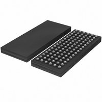
74LVCH32374AEC/LFBGA96/TRAYBDP
Manufacturer
NXP Semiconductors
Series
74LVCHr
Type
D-Type Busr
Datasheet
1.74LVCH32374AEC518.pdf
(13 pages)
Specifications of 74LVCH32374AEC/G:5
Function
Standard
Output Type
Tri-State Non Inverted
Number Of Elements
4
Number Of Bits Per Element
8
Frequency - Clock
150MHz
Delay Time - Propagation
1.5ns
Trigger Type
Positive Edge
Current - Output High, Low
24mA, 24mA
Voltage - Supply
2.7 V ~ 3.6 V
Operating Temperature
-40°C ~ 125°C
Mounting Type
Surface Mount
Package / Case
96-LFBGA
Lead Free Status / RoHS Status
Lead free / RoHS Compliant
Lead Free Status / RoHS Status
Lead free / RoHS Compliant
Other names
74LVCH32374AEC/G-S
74LVCH32374AEC/G-S
935281142551
74LVCH32374AEC/G-S
935281142551
Available stocks
Company
Part Number
Manufacturer
Quantity
Price
Company:

Part Number:
74LVCH32374AEC/G:5
Manufacturer:
NXP Semiconductors
Quantity:
10 000


Philips Semiconductors
FEATURES
DESCRIPTION
The 74LVCH32374A is a high-performance, low-power,
low-voltage, Si-gate CMOS device, superior to most
QUICK REFERENCE DATA
GND = 0 V; T
Notes
1. C
2. The condition is V
2004 May 24
t
t
t
f
C
C
PHL
PZH
PHZ
max
SYMBOL
5 V tolerant inputs/outputs for interfacing with 5 V logic
Wide supply voltage range from 1.2 V to 3.6 V
CMOS low power consumption
MULTIBYTE flow-trough standard pin-out architecture
Low inductance multiple power and ground pins for
minimum noise and ground bounce
Direct interface with TTL levels
All data inputs have bushold
Complies with JEDEC standard JESD8-B/JESD36
ESD protection:
– HBM EIA/JESD22-A114-B exceeds 2000 V
– MM EIA/JESD22-A115-A exceeds 200 V.
Specified from 40 C to +85 C
Packaged in plastic fine-pitch ball grid array package.
I
PD
32-bit edge-triggered D-type flip-flop
with 5 V tolerant inputs/outputs; 3-state
P
f
f
C
V
N = total load switching outputs;
i
o
/t
/t
/t
(C
D
CC
PD
= input frequency in MHz;
L
PLH
PZL
PLZ
= output frequency in MHz;
= output load capacitance in pF;
= C
L
is used to determine the dynamic power dissipation (P
= supply voltage in Volts;
PD
V
CC
amb
propagation delay nCP to nQn
3-state output enable time nOE to nQn C
3-state output disable time nOE to nQn C
maximum clock frequency
input capacitance
power dissipation per flip-flop
2
V
CC
= 25 C; t
f
o
2
) = sum of the outputs.
I
f
= GND to V
i
N + (C
PARAMETER
r
= t
f
2.5 ns
L
CC
.
V
CC
2
f
o
) where:
C
C
V
CC
L
L
L
L
outputs enabled
outputs disabled
= 50 pF; V
= 50 pF; V
= 50 pF; V
= 50 pF; V
2
= 3.3 V; notes 1 and 2
advanced CMOS compatible TTL families.
The inputs can be driven from either 3.3 V or 5 V devices.
In 3-state operation, the outputs can handle 5 V. These
features allow the use of these devices in a mixed
3.3 V or 5 V environment.
The 74LVCH32374A is a 32-bit edge-triggered flip-flop
featuring separate D-type inputs for each flip-flop and
3-state outputs for bus oriented applications. The
74LVCH32374A consists of 4 sections of 8 edge-triggered
flip-flops. A clock (pin nCP) input and an output enable
input (pin nOE) are provided per 8-bit section.
The flip-flops will store the state of their individual D-inputs
that meet the set-up and hold time requirements on the
LOW-to-HIGH nCP transition.
When pin nOE is LOW, the contents of the flip-flops are
available at the outputs. When pin nOE is HIGH, the
outputs go to the high-impedance OFF-state. Operation of
pin nOE does not affect the state of the flip-flops.
The 74LVCH32374A bushold data input circuits eliminate
the need for external pull-up resistors to hold unused
inputs.
D
in W).
CONDITIONS
CC
CC
CC
CC
= 3.3 V
= 3.3 V
= 3.3 V
= 3.3 V
74LVCH32374A
Product specification
3.4
3.5
3.9
150
5.0
19
12
TYPICAL
ns
ns
ns
MHz
pF
pF
pF
UNIT
Related parts for 74LVCH32374AEC/G:5
Image
Part Number
Description
Manufacturer
Datasheet
Request
R

Part Number:
Description:
NXP Semiconductors designed the LPC2420/2460 microcontroller around a 16-bit/32-bitARM7TDMI-S CPU core with real-time debug interfaces that include both JTAG andembedded trace
Manufacturer:
NXP Semiconductors
Datasheet:

Part Number:
Description:
NXP Semiconductors designed the LPC2458 microcontroller around a 16-bit/32-bitARM7TDMI-S CPU core with real-time debug interfaces that include both JTAG andembedded trace
Manufacturer:
NXP Semiconductors
Datasheet:
Part Number:
Description:
NXP Semiconductors designed the LPC2468 microcontroller around a 16-bit/32-bitARM7TDMI-S CPU core with real-time debug interfaces that include both JTAG andembedded trace
Manufacturer:
NXP Semiconductors
Datasheet:
Part Number:
Description:
NXP Semiconductors designed the LPC2470 microcontroller, powered by theARM7TDMI-S core, to be a highly integrated microcontroller for a wide range ofapplications that require advanced communications and high quality graphic displays
Manufacturer:
NXP Semiconductors
Datasheet:
Part Number:
Description:
NXP Semiconductors designed the LPC2478 microcontroller, powered by theARM7TDMI-S core, to be a highly integrated microcontroller for a wide range ofapplications that require advanced communications and high quality graphic displays
Manufacturer:
NXP Semiconductors
Datasheet:
Part Number:
Description:
The Philips Semiconductors XA (eXtended Architecture) family of 16-bit single-chip microcontrollers is powerful enough to easily handle the requirements of high performance embedded applications, yet inexpensive enough to compete in the market for hi
Manufacturer:
NXP Semiconductors
Datasheet:
Part Number:
Description:
The XA-S3 device is a member of Philips Semiconductors? XA(eXtended Architecture) family of high performance 16-bitsingle-chip microcontrollers
Manufacturer:
NXP Semiconductors
Datasheet:

Part Number:
Description:
The NXP BlueStreak LH75401/LH75411 family consists of two low-cost 16/32-bit System-on-Chip (SoC) devices
Manufacturer:
NXP Semiconductors
Datasheet:
Part Number:
Description:
The NXP LPC3130/3131 combine an 180 MHz ARM926EJ-S CPU core, high-speed USB2
Manufacturer:
NXP Semiconductors
Datasheet:
Part Number:
Description:
The NXP LPC3141 combine a 270 MHz ARM926EJ-S CPU core, High-speed USB 2
Manufacturer:
NXP Semiconductors
Part Number:
Description:
The NXP LPC3143 combine a 270 MHz ARM926EJ-S CPU core, High-speed USB 2
Manufacturer:
NXP Semiconductors

Part Number:
Description:
The NXP LPC3152 combines an 180 MHz ARM926EJ-S CPU core, High-speed USB 2
Manufacturer:
NXP Semiconductors
Part Number:
Description:
The NXP LPC3154 combines an 180 MHz ARM926EJ-S CPU core, High-speed USB 2
Manufacturer:
NXP Semiconductors

Part Number:
Description:
Standard level N-channel enhancement mode Field-Effect Transistor (FET) in a plastic package using NXP High-Performance Automotive (HPA) TrenchMOS technology
Manufacturer:
NXP Semiconductors
Datasheet: