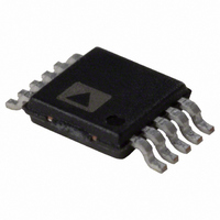
AD5324BRM Analog Devices Inc, AD5324BRM Datasheet - Page 18

AD5324BRM
Manufacturer Part Number
AD5324BRM
Description
Digital/Analog Converter IC Interface Type:Serial
Manufacturer
Analog Devices Inc
Datasheet
1.AD5304ARMZ-REEL7.pdf
(24 pages)
Specifications of AD5324BRM
Number Of Bits
12
Number Of Outputs
4
Package/case
10-SOIC
A/d, D/a Features
2.5 V To 5.5 V, 500 A Quad Voltage Output 12-Bit DAC
Mounting Type
Surface Mount
Rohs Status
RoHS non-compliant
Settling Time
6µs
Data Interface
Serial
Number Of Converters
4
Voltage Supply Source
Single Supply
Power Dissipation (max)
5mW
Operating Temperature
-40°C ~ 105°C
Package / Case
10-MSOP, Micro10™, 10-uMAX, 10-uSOP
Lead Free Status / RoHS Status
Available stocks
Company
Part Number
Manufacturer
Quantity
Price
Part Number:
AD5324BRMZ
Manufacturer:
ADI/亚德诺
Quantity:
20 000
Part Number:
AD5324BRMZ-REEL7
Manufacturer:
ADI/亚德诺
Quantity:
20 000
AD5304/AD5314/AD5324
APPLICATIONS
TYPICAL APPLICATION CIRCUIT
The AD5304/AD5314/AD5324 can be used with a wide range
of reference voltages where the devices offer full, one-quadrant
multiplying capability over a reference range of 0 V to V
More typically, these devices are used with a fixed, precision
reference voltage. Suitable references for 5 V operation are the
AD780 and REF192 (2.5 V references). For 2.5 V operation, a
suitable external reference would be the AD589, a 1.23 V band
gap reference. Figure 40 shows a typical setup for the AD5304/
AD5314/AD5324 when using an external reference.
If an output range of 0 V to V
to connect the reference input to V
accurate and can be noisy, the AD5304/AD5314/ AD5324 can
be powered from the reference voltage; for example, using a 5 V
reference such as the REF195. The REF195 can output a steady
supply voltage for the AD5304/ AD5314/AD5324. The current
required from the REF195 is 600 μA supply current and approxi-
mately 112 μA into the reference input. This is with no load on
the DAC outputs. When the DAC outputs are loaded, the REF195
also needs to supply the current to the loads. The total current
required (with a 10 kΩ load on each output) is
The load regulation of the REF195 is typically 2 ppm/mA, resulting
in an error of 5.4 ppm (27 μV) for the 2.7 mA current drawn from
it. This corresponds to a 0.0014 LSB error at eight bits and 0.022
LSB error at 12 bits.
712 μA + 4 (5 V/10 kΩ) = 2.70 mA
OR AD589 WITH
AD790/REF192
WITH V
V
REFERENCE
Figure 40. AD5304/AD5314/AD5324 Using External Reference
EXTERNAL
IN
V
DD
= 2.5V
DD
V
OUT
= 5V
0.1µF
1µF
INTERFACE
SERIAL
DD
10µF
is required, the simplest solution is
REFIN
SCLK
DIN
SYNC
DD
AD5304/AD5314/
V
. As this supply is not very
DD
A0
= 2.5V TO 5.5V
AD5324
GND
V
V
V
V
OUT
OUT
OUT
OUT
A
B
C
D
DD
.
Rev. F | Page 18 of 24
Bipolar Operation Using the AD5304/AD5314/AD5324
The AD5304/AD5314/AD5324 have been designed for single
supply operation, but a bipolar output range is also possible
using the circuit in Figure 41. This circuit gives an output voltage
range of ±5 V. Rail-to-rail operation at the amplifier output is
achievable using an AD820 or an OP295 as the output amplifier.
The output voltage for any input code can be calculated as follows:
where:
D is the decimal equivalent of the code loaded to the DAC.
N is the DAC resolution.
REFIN is the reference voltage input:
V
+6V TO +16V
OUT
10µF
V
IN
REF195
=
REFIN = 5 V, R1 = R2 = 10 kΩ
V
GND
OUT
⎡
⎢
⎢
⎣
(
V
0.1µF
REFIN
OUT
= (10 × D /2
Figure 41. Bipolar Operation with the AD5304
×
+5V
1µF
D
2 /
R1
N
) − 5 V
V
REFIN
GND
N
DD
DIN
)
×
INTERFACE
R1 = 10kΩ
AD5304
(
SERIAL
R1
SCLK SYNC
+
R2
V
V
V
V
OUT
OUT
OUT
OUT
)
⎤
⎥
⎥
⎦
A
B
C
D
−
REFIN
R2 = 10kΩ
AD820/
OP295
+5V
–5V
×
(
R
/ 2
R
±5V
) 1


