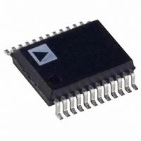
ADE7755ARSZRL Analog Devices Inc, ADE7755ARSZRL Datasheet - Page 11

ADE7755ARSZRL
Manufacturer Part Number
ADE7755ARSZRL
Description
Energy Metering IC With Pulse Output
Manufacturer
Analog Devices Inc
Datasheet
1.ADE7755ARSZRL.pdf
(20 pages)
Specifications of ADE7755ARSZRL
Input Impedance
390 KOhm
Measurement Error
0.1%
Voltage - I/o High
2.4V
Voltage - I/o Low
0.8V
Current - Supply
3mA
Voltage - Supply
4.75 V ~ 5.25 V
Operating Temperature
-40°C ~ 85°C
Mounting Type
Surface Mount
Package / Case
24-SSOP (0.200", 5.30mm Width)
Meter Type
Single Phase
Lead Free Status / RoHS Status
Lead free / RoHS Compliant
For Use With
EVAL-ADE7755ZEB - BOARD EVALUATION FOR AD7755
Lead Free Status / RoHS Status
Lead free / RoHS Compliant
Available stocks
Company
Part Number
Manufacturer
Quantity
Price
Company:
Part Number:
ADE7755ARSZRL
Manufacturer:
FREESCALE
Quantity:
430
TERMINOLOGY
Measurement Error
The error associated with the energy measurement made by the
ADE7755 is defined by the following formula:
Phase Error Between Channels
The high-pass filter (HPF) in Channel 1 has a phase lead response.
To offset this phase response and equalize the phase response
between channels, a phase compensation network is also placed
in Channel 1. The phase compensation network matches the
phase to within ±0.1° over a range of 45 Hz to 65 Hz and ±0.2°
over a range of 40 Hz to 1 kHz. See Figure 30 and Figure 31.
Power Supply Rejection (PSR)
The PSR quantifies the ADE7755 measurement error as a
percentage of the reading when the power supplies are varied.
For the ac PSR measurement, a reading at nominal supplies
(5 V) is taken. A 200 mV rms/100 Hz signal is then introduced
onto the supplies and a second reading is obtained under the
same input signal levels. Any error introduced is expressed as a
percentage of the reading (see the Measurement Error definition).
For the dc PSR measurement, a reading at nominal supplies
(5 V) is taken. The supplies are then varied ±5% and a second
reading is obtained with the same input signal levels. Any error
introduced is again expressed as a percentage of the reading.
Percentage
Energy
Registered
Error
=
by
True
the
Energy
ADE
7755
−
True
Energy
×
100
%
Rev. A | Page 11 of 20
ADC Offset Error
The ADC offset error refers to the dc offset associated with the
analog inputs to the ADCs. It means that with the analog inputs
connected to AGND, the ADCs still see a small dc signal
(offset). The offset decreases with increasing gain in Channel 1.
This specification is measured at a gain of 1. At a gain of 16, the
dc offset is typically less than 1 mV. However, when the HPF is
switched on, the offset is removed from the current channel,
and the power calculation is not affected by this offset.
Gain Error
The gain error of the ADE7755 is defined as the difference between
the measured output frequency (minus the offset) and the ideal
output frequency. It is measured with a gain of 1 in Channel 1.
The difference is expressed as a percentage of the ideal frequency.
The ideal frequency is obtained from the ADE7755 transfer
function (see the Transfer Function section).
Gain Error Match
The gain error match is defined as the gain error (minus the
offset) obtained when switching between a gain of 1 and a gain
of 2, 8, or 16. It is expressed as a percentage of the output frequency
obtained under a gain of 1. This gives the gain error observed
when the gain selection is changed from 1 to 2, 8, or 16.
ADE7755


