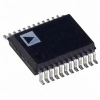
ADE7755ARSZRL Analog Devices Inc, ADE7755ARSZRL Datasheet - Page 4

ADE7755ARSZRL
Manufacturer Part Number
ADE7755ARSZRL
Description
Energy Metering IC With Pulse Output
Manufacturer
Analog Devices Inc
Datasheet
1.ADE7755ARSZRL.pdf
(20 pages)
Specifications of ADE7755ARSZRL
Input Impedance
390 KOhm
Measurement Error
0.1%
Voltage - I/o High
2.4V
Voltage - I/o Low
0.8V
Current - Supply
3mA
Voltage - Supply
4.75 V ~ 5.25 V
Operating Temperature
-40°C ~ 85°C
Mounting Type
Surface Mount
Package / Case
24-SSOP (0.200", 5.30mm Width)
Meter Type
Single Phase
Lead Free Status / RoHS Status
Lead free / RoHS Compliant
For Use With
EVAL-ADE7755ZEB - BOARD EVALUATION FOR AD7755
Lead Free Status / RoHS Status
Lead free / RoHS Compliant
Available stocks
Company
Part Number
Manufacturer
Quantity
Price
Company:
Part Number:
ADE7755ARSZRL
Manufacturer:
FREESCALE
Quantity:
430
ADE7755
Parameter
POWER SUPPLY
1
2
3
TIMING CHARACTERISTICS
AV
Table 2.
Parameter
t
t
t
t
t
t
1
2
3
4
1
2
3
4
5
6
See the Terminology section.
See the Typical Performance Characteristics section for the plots.
Sample tested during initial release and after any redesign or process change that may affect this parameter.
Sample tested during initial release and after any redesign or process change that may affect this parameter.
See Figure 2.
The pulse widths of F1, F2, and CF are not fixed for higher output frequencies. See the Frequency Outputs section.
The CF pulse is always 18 μs in the high frequency mode. See the Frequency Outputs section and Table 8.
3, 4
3
AV
DV
AI
DI
DD
DD
DD
DD
DD
= DV
1, 2
DD
= 5 V ± 5%, AGND = DGND = 0 V, on-chip reference, CLKIN = 3.58 MHz, T
Specification
275
See Table 7
1/2 t
90
See Table 8
CLKIN/4
2
CF
F1
F2
t
4
Min
4.75
4.75
t
1
Figure 2. Timing Diagram for Frequency Outputs
Unit
ms
sec
sec
ms
sec
sec
t
3
t
Typ
6
t
5
Rev. A | Page 4 of 20
t
2
Max
5.25
5.25
3
2.5
Test Conditions/Comments
F1 and F2 pulse width (logic low)
Output pulse period; see the Transfer Function section
Time between F1 falling edge and F2 falling edge
CF pulse width (logic high)
CF pulse period; see the Transfer Function section
Minimum time between F1 and F2 pulse
Unit
V
V
V
V
mA
mA
Test Conditions/Comments
For specified performance
5 V − 5%
5 V + 5%
5 V − 5%
5 V + 5%
Typically 2 mA
Typically 1.5 mA
MIN
to T
MAX
= −40°C to +85°C.


