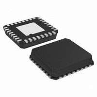
ADG2188YCPZ-HS-RL7 Analog Devices Inc, ADG2188YCPZ-HS-RL7 Datasheet

ADG2188YCPZ-HS-RL7
Specifications of ADG2188YCPZ-HS-RL7
Available stocks
Related parts for ADG2188YCPZ-HS-RL7
ADG2188YCPZ-HS-RL7 Summary of contents
Page 1
FEATURES 2 I C-compatible interface 2 3.4 MHz high speed I C option 32-lead LFCSP_VQ (5 mm × 5 mm) Double-buffered input logic Simultaneous update of multiple switches Up to 300 MHz bandwidth Fully specified at dual ±5 V/single +12 ...
Page 2
ADG2188 TABLE OF CONTENTS Features .............................................................................................. 1 Applications....................................................................................... 1 General Description ......................................................................... 1 Functional Block Diagram .............................................................. 1 Revision History ............................................................................... 2 Specifications..................................................................................... Timing Specifications............................................................ 7 Timing Diagram ........................................................................... 8 Absolute Maximum Ratings............................................................ 9 ESD Caution.................................................................................. ...
Page 3
SPECIFICATIONS ± 10 GND = 0 V, all specifications Table 1. Parameter +25°C ANALOG SWITCH Analog Signal Range On Resistance ...
Page 4
ADG2188 Parameter +25°C 2 LOGIC INPUTS (SCL, SDA) Input High Voltage, V INH Input Low Voltage, V INL Input Leakage Current, I 0.005 IN Input Hysteresis Input Capacitance LOGIC OUTPUT (SDA) Output Low Voltage ...
Page 5
± 10 −5 V ± 10 Table 2. Parameter +25°C ANALOG SWITCH Analog Signal Range On Resistance Resistance Matching 4.5 ...
Page 6
ADG2188 Parameter +25°C Input Hysteresis Input Capacitance LOGIC OUTPUT (SDA) Output Low Voltage Floating State Leakage Current POWER REQUIREMENTS Interface Inactive 0.3 Interface Active: 400 kHz ...
Page 7
I C TIMING SPECIFICATIONS − Table 3. 1 Parameter Conditions f Standard mode SCL Fast mode 2 High speed mode C = ...
Page 8
ADG2188 1 Parameter Conditions t Standard mode 11 Fast mode 2 High speed mode C = 100 pF maximum 400 pF maximum B t Standard mode 11A Fast mode 2 High speed mode C = 100 pF ...
Page 9
ABSOLUTE MAXIMUM RATINGS T = 25°C, unless otherwise noted. A Table 4. Parameter Rating GND −0 + GND +0 − ...
Page 10
ADG2188 PIN CONFIGURATION AND FUNCTION DESCRIPTIONS 1 Table 5. Pin Function Descriptions Pin No. Mnemonic Description 1 V Negative Power Supply in a Dual-Supply Application. For single-supply applications, this pin should be tied to GND ...
Page 11
TYPICAL PERFORMANCE CHARACTERISTICS 200 T = 25° 10mA 180 DS 160 140 V = –5V 120 +5V DD 100 –5 –4 –3 –2 – ...
Page 12
ADG2188 10mA +85° –40° 0.5 1.0 1.5 2.0 2.5 SOURCE VOLTAGE (V) Figure ...
Page 13
OFF 200 V = +5V –5V 180 160 V = 12V 140 120 100 –40 – TEMPERATURE (°C) Figure 16. t ...
Page 14
ADG2188 0. + –5V SS 0.30 0.25 0.20 0.15 0.10 0. 0.5 1.0 1.5 FREQUENCY (MHz) Figure 22. Digital Current (I ) vs. Frequency L 1.8 1.6 1 1.2 ...
Page 15
TEST CIRCUITS The test circuits show measurements on one channel for clarity, but the circuit applies to any of the switches in the matrix V1 Figure 25. On Resistance ...
Page 16
ADG2188 V DD 0.1µF NETWORK ANALYZER OUT 50Ω X2 50Ω DATA V X BIT GND V OUT CHANNEL-TO-CHANNEL CROSSTALK = 20 log V Figure 32. Channel-to-Channel Crosstalk V SS 0.1µ ...
Page 17
TERMINOLOGY On Resistance ( The series on-channel resistance measured between the X input/output and the Y input/output. On Resistance Match (Δ The channel-to-channel matching of on resistance when channels are operated under identical conditions. On Resistance ...
Page 18
ADG2188 THEORY OF OPERATION The ADG2188 is an analog cross point switch with an array size of 8 × 8. The eight rows are referred to as the X input/output lines, and the eight columns are referred to as the ...
Page 19
SERIAL INTERFACE 2 The ADG2188 is controlled via an I C-compatible serial bus. The parts are connected to this bus as a slave device (no clock is generated by the switch). 2 HIGH SPEED I C INTERFACE In addition to ...
Page 20
ADG2188 WRITING TO THE ADG2188 INPUT SHIFT REGISTER The input shift register is 24 bits wide. A 3-byte write is necessary when writing to this register and is done under the control of the serial clock input, SCL. The contents ...
Page 21
DB15 DB14 DB13 DB12 DATA AX3 AX2 AX1 ...
Page 22
ADG2188 WRITE OPERATION When writing to the ADG2188, the user must begin with an address byte and R/ W bit, after which the switch acknowledges that it is prepared to receive data by pulling SDA low. This address byte is ...
Page 23
SCL SDA START ADDRESS BYTE COND BY MASTER SCL A2 A1 SDA A0 START ADDRESS BYTE COND BY MASTER R/W RB7 RB6 RB5 RB4 RB3 RB2 RB1 ACK DATA BYTE BY SWITCH R/W ACK DUMMY READBACK BYTE ...
Page 24
ADG2188 EVALUATION BOARD The ADG2188 evaluation board allows designers to evaluate the high performance 8 × 8 switch array of the ADG2188 with a minimum of effort. The evaluation kit includes a populated, tested ADG2188 printed circuit board. The evaluation ...
Page 25
SCHEMATICS Figure 36. EVAL-ADG2188EB Schematic, USB Controller Section Rev Page ADG2188 ...
Page 26
ADG2188 Figure 37. EVAL-ADG2188EB Schematic, Chip Section Rev Page ...
Page 27
... ADG2188BCPZ-REEL7 1 −40°C to +85°C 1 ADG2188BCPZ-HS-RL7 −40°C to +85°C 1 ADG2188YCPZ-R2 −40°C to +125°C 1 ADG2188YCPZ-REEL7 −40°C to +125°C 1 ADG2188YCPZ-HS-RL7 −40°C to +125°C EVAL-ADG2188EB Pb-free part. 5.00 BSC SQ 0.60 MAX 24 0.50 BSC TOP 4.75 VIEW BSC SQ 0 ...
Page 28
ADG2188 NOTES 2 Purchase of licensed I C components of Analog Devices or one of its sublicensed Associated Companies conveys a license for the purchaser under the Philips I Rights to use these components system, ...


