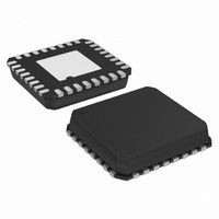
ADG2188YCPZ-HS-RL7 Analog Devices Inc, ADG2188YCPZ-HS-RL7 Datasheet - Page 22

ADG2188YCPZ-HS-RL7
Manufacturer Part Number
ADG2188YCPZ-HS-RL7
Description
IC,ANALOG SWITCH,SINGLE,8X8 CROSSPOINT,CMOS,LLCC,32PIN,PLASTIC
Manufacturer
Analog Devices Inc
Series
I²Cr
Datasheet
1.ADG2188YCPZ-HS-RL7.pdf
(28 pages)
Specifications of ADG2188YCPZ-HS-RL7
Function
Crosspoint Switch
Circuit
1 x 8:8
On-state Resistance
50 Ohm
Voltage Supply Source
Single Supply
Voltage - Supply, Single/dual (±)
12V, 15V
Current - Supply
.05µA
Operating Temperature
-40°C ~ 125°C
Mounting Type
Surface Mount
Package / Case
32-VFQFN, CSP Exposed Pad
Lead Free Status / RoHS Status
Lead free / RoHS Compliant
For Use With
EVAL-ADG2188EBZ - BOARD EVAL FOR ADG2188
Lead Free Status / RoHS Status
Lead free / RoHS Compliant
Other names
ADG2188YCPZ-HS-RL7TR
Available stocks
Company
Part Number
Manufacturer
Quantity
Price
Company:
Part Number:
ADG2188YCPZ-HS-RL7
Manufacturer:
Maxim
Quantity:
101
ADG2188
WRITE OPERATION
When writing to the ADG2188, the user must begin with an
address byte and R/ W bit, after which the switch acknowledges
that it is prepared to receive data by pulling SDA low. This
address byte is followed by the two 8-bit words. The write
operations for the switch array are shown in Figure 34. Note
that it is only the condition of the switch corresponding to the
bits in the data bytes that changes state. All other switches retain
their previous condition.
READ OPERATION
Readback on the ADG2188 is designed to work as a tool for
debug and can be used to output the status of any of the
64 switches of the device. The readback function is a two-step
sequence that works as follows:
1.
SDA
Table 8. Readback Addresses for Each X Line
X Line
X0
X1
X2
X3
X4
X5
X6
X7
SCL
MASTER
a.
START
Select the relevant X line to be read back from. Note that
there are eight switches connecting that X line to the eight
Y lines. The next step involves writing to the ADG2188 to
tell the part to reveal the status of those eight switches.
COND
BY
Enter the I
R/ W to 0 to indicate a write to the device.
ADDRESS BYTE
RB7
0
0
0
0
0
0
0
0
2
C address of the ADG2188, and set the
A2
A1
RB6
0
0
1
1
0
0
1
1
A0
R/W
SWITCH
ACK
BY
DATA
RB5
1
1
1
1
1
1
1
1
AX3
AX2
Figure 34. Write Operation
Rev. 0 | Page 22 of 28
AX1
DATA BYTE
RB4
1
1
1
1
1
1
1
1
AX0
AY2
2.
The entire read sequence is shown in Figure 35.
AY1
b.
c.
d.
The second step involves reading back from the register
that holds the status of the eight switches associated with
the X line of choice.
a. As before, enter the I
AY0
RB3
0
1
0
1
0
1
0
1
SWITCH
Enter the readback address for the X line of interest,
the addresses of which are shown in Table 8. Note that
the ADG2188 is expecting a 2-byte write; therefore, be
sure to also enter another byte of don’t cares (see
Figure 35).
The ADG2188 then places the status of those eight
switches in a register than can be read back.
time, set the R/ W to 1 to indicate a read back from the
device.
As with a write to the device, the ADG2188 outputs a
2-byte sequence during readback. Therefore, the first
eight bits of data out that are read back are all 0s. The
next eight bits of data that come back are the status of
the eight Y lines attached to that particular X line. If
the bit is a 1, then the switch is closed (on); similarly, if
the bit is a 0, the switch is open (off).
ACK
BY
x
x
RB2
1
1
1
1
1
1
1
1
x
x
2
DATA BYTE
C address of the ADG2188. This
x
RB1
0
0
0
0
0
0
0
0
x
x
LDSW
SWITCH
ACK
BY
RB0
0
0
0
0
1
1
1
1
MASTER
COND
STOP
BY


