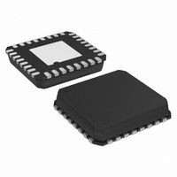
ADG2188YCPZ-HS-RL7 Analog Devices Inc, ADG2188YCPZ-HS-RL7 Datasheet - Page 19

ADG2188YCPZ-HS-RL7
Manufacturer Part Number
ADG2188YCPZ-HS-RL7
Description
IC,ANALOG SWITCH,SINGLE,8X8 CROSSPOINT,CMOS,LLCC,32PIN,PLASTIC
Manufacturer
Analog Devices Inc
Series
I²Cr
Datasheet
1.ADG2188YCPZ-HS-RL7.pdf
(28 pages)
Specifications of ADG2188YCPZ-HS-RL7
Function
Crosspoint Switch
Circuit
1 x 8:8
On-state Resistance
50 Ohm
Voltage Supply Source
Single Supply
Voltage - Supply, Single/dual (±)
12V, 15V
Current - Supply
.05µA
Operating Temperature
-40°C ~ 125°C
Mounting Type
Surface Mount
Package / Case
32-VFQFN, CSP Exposed Pad
Lead Free Status / RoHS Status
Lead free / RoHS Compliant
For Use With
EVAL-ADG2188EBZ - BOARD EVAL FOR ADG2188
Lead Free Status / RoHS Status
Lead free / RoHS Compliant
Other names
ADG2188YCPZ-HS-RL7TR
Available stocks
Company
Part Number
Manufacturer
Quantity
Price
Company:
Part Number:
ADG2188YCPZ-HS-RL7
Manufacturer:
Maxim
Quantity:
101
SERIAL INTERFACE
The ADG2188 is controlled via an I
The parts are connected to this bus as a slave device (no clock
is generated by the switch).
HIGH SPEED I
In addition to standard and full speed I
supports the high speed (3.4 MHz) I
models provide this added performance. See the Ordering
Guide for details.
SERIAL BUS ADDRESS
The ADG2188 has a 7-bit slave address. The four MSBs are
hard coded to 1110, and the three LSBs are determined by the
state of Pin A0, Pin A1, and Pin A2. By offering the facility to
hardware configure Pin A0, Pin A1, and Pin A2, up to eight
of these devices can be connected to a single serial bus.
The 2-wire serial bus protocol operates as follows:
1.
The master initiates data transfer by establishing a start
condition, defined as when a high-to-low transition on
the SDA line occurs while SCL is high. This indicates
that an address/data stream follows. All slave peripherals
connected to the serial bus respond to the start condition
and shift in the next eight bits, consisting of a 7-bit
address (MSB first) plus an R/ W bit that determines the
direction of the data transfer, that is, whether data is
written to or read from the slave device.
2
C INTERFACE
2
C-compatible serial bus.
2
C interface. Only the –HS
2
C, the ADG2188 also
Rev. 0 | Page 19 of 28
2.
3.
4.
Refer to Figure 33 and Figure 34 for a graphical explanation
of the serial data transfer protocol.
When all data bits have been read or written, a stop
The peripheral whose address corresponds to the trans-
mitted address responds by pulling the SDA line low
during the ninth clock pulse, known as the acknowledge
bit. At this stage, all other devices on the bus remain idle
while the selected device waits for data to be written to
or read from its serial register. If the R/ W bit is 1 (high), the
master reads from the slave device. If the R/ W bit is 0
(low), the master writes to the slave device.
Data is transmitted over the serial bus in sequences of
nine clock pulses: eight data bits followed by an acknowl-
edge bit from the receiver of the data. Transitions on the
SDA line must occur during the low period of the clock
signal, SCL, and remain stable during the high period of
SCL, because a low-to-high transition when the clock is
high can be interpreted as a stop signal.
condition is established by the master. A stop condition
is defined as a low-to-high transition on the SDA line
while SCL is high. In write mode, the master pulls the
SDA line high during the 10th clock pulse to establish a
stop condition. In read mode, the master issues a no
acknowledge for the ninth clock pulse (that is, the SDA
line remains high). The master then brings the SDA line
low before the 10th clock pulse and then high during the
10th clock pulse to establish a stop condition.
ADG2188


