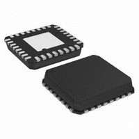
ADG2188YCPZ-HS-RL7 Analog Devices Inc, ADG2188YCPZ-HS-RL7 Datasheet - Page 10

ADG2188YCPZ-HS-RL7
Manufacturer Part Number
ADG2188YCPZ-HS-RL7
Description
IC,ANALOG SWITCH,SINGLE,8X8 CROSSPOINT,CMOS,LLCC,32PIN,PLASTIC
Manufacturer
Analog Devices Inc
Series
I²Cr
Datasheet
1.ADG2188YCPZ-HS-RL7.pdf
(28 pages)
Specifications of ADG2188YCPZ-HS-RL7
Function
Crosspoint Switch
Circuit
1 x 8:8
On-state Resistance
50 Ohm
Voltage Supply Source
Single Supply
Voltage - Supply, Single/dual (±)
12V, 15V
Current - Supply
.05µA
Operating Temperature
-40°C ~ 125°C
Mounting Type
Surface Mount
Package / Case
32-VFQFN, CSP Exposed Pad
Lead Free Status / RoHS Status
Lead free / RoHS Compliant
For Use With
EVAL-ADG2188EBZ - BOARD EVAL FOR ADG2188
Lead Free Status / RoHS Status
Lead free / RoHS Compliant
Other names
ADG2188YCPZ-HS-RL7TR
Available stocks
Company
Part Number
Manufacturer
Quantity
Price
Company:
Part Number:
ADG2188YCPZ-HS-RL7
Manufacturer:
Maxim
Quantity:
101
ADG2188
PIN CONFIGURATION AND FUNCTION DESCRIPTIONS
Table 5. Pin Function Descriptions
Pin No.
1
2, 19 to 23
3 to 8,
17, 18
9 to 16
24
25
26
27
28
29
30
31
32
1
It is recommended that the exposed paddle be soldered to V
Mnemonic
V
NC
X0 to X7
Y0 to Y7
V
V
SDA
SCL
A0
A1
A2
RESET
GND
SS
DD
L
Description
Negative Power Supply in a Dual-Supply Application. For single-supply applications, this pin should be tied to GND.
No Connect.
Can be inputs or outputs.
Can be inputs or outputs.
Positive Power Supply Input.
Logic Power Supply Input.
Digital I/O. Bidirectional open drain data line. External pull-up resistor required.
Digital Input, Serial Clock Line. Open drain input that is used in conjunction with SDA to clock data into the
device. External pull-up resistor required.
Logic Input. Address pin that sets the least significant bit of the 7-bit slave address.
Logic Input. Address pin that sets the second least significant bit of the 7-bit slave address.
Logic Input. Address pin that sets the third least significant bit of the 7-bit slave address.
Active Low Logic Input. When this pin is low, all switches are open, and appropriate registers are cleared to 0.
Ground. Reference point for all circuitry on the ADG2188.
1
V
NC
X0
X1
X2
X3
X4
X5
SS
Exposed Paddle Soldered to V
NC = NO CONNECT
SS
to improve heat dissipation and crosstalk.
1
2
3
4
5
6
7
8
32
9
Figure 3. Pin Configuration
31
10
PIN 1
INDICATOR
Rev. 0 | Page 10 of 28
30
11
(Not to Scale)
ADG2188
TOP VIEW
12
29
8 × 8
13
28
14
27
15
26
SS
16
25
24
23
22
21
20
19
18
17
V
NC
NC
NC
NC
NC
X7
X6
DD


