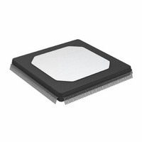
ADSP-21060KS-160 Analog Devices Inc, ADSP-21060KS-160 Datasheet - Page 22

ADSP-21060KS-160
Manufacturer Part Number
ADSP-21060KS-160
Description
Digital Signal Processor IC
Manufacturer
Analog Devices Inc
Series
SHARC®r
Type
Floating Pointr
Datasheets
1.ADSP-21062KSZ-133.pdf
(64 pages)
2.ADSP-21060KS-160.pdf
(47 pages)
3.ADSP-21060KS-160.pdf
(64 pages)
Specifications of ADSP-21060KS-160
Supply Voltage Max
5.25V
Dsp Type
Fixed / Floating Point
Mounting Type
Surface Mount
Package / Case
240-MQFP
Memory Organization - Ram
4M
Rohs Status
RoHS non-compliant
Interface
Host Interface, Link Port, Serial Port
Clock Rate
40MHz
Non-volatile Memory
External
On-chip Ram
512kB
Voltage - I/o
5.00V
Voltage - Core
5.00V
Operating Temperature
0°C ~ 85°C
Device Core Size
32b
Architecture
Super Harvard
Format
Floating Point
Clock Freq (max)
40MHz
Mips
40
Device Input Clock Speed
40MHz
Ram Size
512KB
Operating Supply Voltage (typ)
5V
Operating Supply Voltage (min)
4.75V
Operating Supply Voltage (max)
5.25V
Operating Temp Range
0C to 85C
Operating Temperature Classification
Commercial
Mounting
Surface Mount
Pin Count
240
Package Type
MQFP
Lead Free Status / Rohs Status
Not Compliant
Available stocks
Company
Part Number
Manufacturer
Quantity
Price
Company:
Part Number:
ADSP-21060KS-160
Manufacturer:
AD
Quantity:
5 510
Company:
Part Number:
ADSP-21060KS-160
Manufacturer:
SHARP
Quantity:
5 510
Company:
Part Number:
ADSP-21060KS-160
Manufacturer:
Analog Devices Inc
Quantity:
10 000
ADSP-21060/ADSP-21060L/ADSP-21062/ADSP-21062L/ADSP-21060C/ADSP-21060LC
Clock Input
Table 9. Clock Input
1
Reset
Table 10. Reset
1
2
Parameter
Timing Requirements
t
t
t
t
Parameter
Timing Requirements
t
t
For the ADSP-21060LC, this specification is 9.5 ns min.
Applies after the power-up sequence is complete. At power-up, the processor’s internal phase-locked loop requires no more than 100 μs while RESET is low, assuming stable
Only required if multiple ADSP-2106xs must come out of reset synchronous to CLKIN with program counters (PC) equal. Not required for multiple ADSP-2106xs commu-
CK
CKL
CKH
CKRF
WRST
SRST
V
nicating over the shared bus (through the external port), because the bus arbitration logic automatically synchronizes itself after reset.
DD
and CLKIN (not including start-up time of external clock oscillator).
CLKIN Period
CLKIN Width Low
CLKIN Width High
CLKIN Rise/Fall (0.4 V to 2.0 V)
RESET Pulse Width Low
RESET Setup Before CLKIN High
RESET
CLKIN
CLKIN
1
Min
7
5
25
ADSP-21060
ADSP-21062
40 MHz, 5 V
2
Rev. F | Page 22 of 64 | March 2008
Max
100
3
Figure 9. Clock Input
Figure 10. Reset
t
CKH
Min
30
7
5
ADSP-21060
ADSP-21062
33 MHz, 5 V
t
WRST
Max
100
3
t
t
CK
CKL
Min
4t
14 + DT/2
CK
Min
25
8.75
5
ADSP-21060L
ADSP-21062L
40 MHz, 3.3 V
t
SRST
5 V and 3.3 V
Max
100
3
Max
t
CK
30
Min
8.75
5
ADSP-21060L
ADSP-21062L
33 MHz, 3.3 V
1
Max
100
3
Unit
ns
ns
Unit
ns
ns
ns
ns


