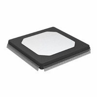
ADSP-21060KS-160 Analog Devices Inc, ADSP-21060KS-160 Datasheet - Page 34

ADSP-21060KS-160
Manufacturer Part Number
ADSP-21060KS-160
Description
Digital Signal Processor IC
Manufacturer
Analog Devices Inc
Series
SHARC®r
Type
Floating Pointr
Datasheets
1.ADSP-21062KSZ-133.pdf
(64 pages)
2.ADSP-21060KS-160.pdf
(47 pages)
3.ADSP-21060KS-160.pdf
(64 pages)
Specifications of ADSP-21060KS-160
Supply Voltage Max
5.25V
Dsp Type
Fixed / Floating Point
Mounting Type
Surface Mount
Package / Case
240-MQFP
Memory Organization - Ram
4M
Rohs Status
RoHS non-compliant
Interface
Host Interface, Link Port, Serial Port
Clock Rate
40MHz
Non-volatile Memory
External
On-chip Ram
512kB
Voltage - I/o
5.00V
Voltage - Core
5.00V
Operating Temperature
0°C ~ 85°C
Device Core Size
32b
Architecture
Super Harvard
Format
Floating Point
Clock Freq (max)
40MHz
Mips
40
Device Input Clock Speed
40MHz
Ram Size
512KB
Operating Supply Voltage (typ)
5V
Operating Supply Voltage (min)
4.75V
Operating Supply Voltage (max)
5.25V
Operating Temp Range
0C to 85C
Operating Temperature Classification
Commercial
Mounting
Surface Mount
Pin Count
240
Package Type
MQFP
Lead Free Status / Rohs Status
Not Compliant
Available stocks
Company
Part Number
Manufacturer
Quantity
Price
Company:
Part Number:
ADSP-21060KS-160
Manufacturer:
AD
Quantity:
5 510
Company:
Part Number:
ADSP-21060KS-160
Manufacturer:
SHARP
Quantity:
5 510
Company:
Part Number:
ADSP-21060KS-160
Manufacturer:
Analog Devices Inc
Quantity:
10 000
ADSP-21060/ADSP-21060L/ADSP-21062/ADSP-21062L/ADSP-21060C/ADSP-21060LC
Three-State Timing—Bus Master/ Bus Slave
These specifications show how the memory interface is disabled
(stops driving) or enabled (resumes driving) relative to CLKIN
and the SBTS pin. This timing is applicable to bus master transi-
tion cycles (BTC) and host transition cycles (HTC) as well as the
SBTS pin.
Table 21. Three-State Timing—Bus Master, Bus Slave
1
2
3
4
5
Parameter
Timing Requirements
t
t
Switching Characteristics
t
t
t
t
t
t
t
t
t
t
t
t
t
t
For ADSP-21060L/ADSP-21060LC/ADSP-21062L, specification is –1.25 – DT/8 ns min, for ADSP-21062, specification is –1 – DT/8 ns min.
Strobes = RD, WR, PAGE, DMAG, BMS, SW.
For ADSP-21060LC, specification is 0.25 – DT/4 ns max.
In addition to bus master transition cycles, these specs also apply to bus master and bus slave synchronous read/write.
Memory Interface = Address, RD, WR, MSx, SW, PAGE, DMAGx, and BMS (in EPROM boot mode).
STSCK
HTSCK
MIENA
MIENS
MIENHG
MITRA
MITRS
MITRHG
DATEN
DATTR
ACKEN
ACKTR
ADCEN
ADCTR
MTRHBG
MENHBG
INTERFACE
MEMORY
HBG
SBTS Setup Before CLKIN
SBTS Hold Before CLKIN
Address/Select Enable After CLKIN
Strobes Enable After CLKIN
HBG Enable After CLKIN
Address/Select Disable After CLKIN
Strobes Disable After CLKIN
HBG Disable After CLKIN
Data Enable After CLKIN
Data Disable After CLKIN
ACK Enable After CLKIN
ACK Disable After CLKIN
ADRCLK Enable After CLKIN
ADRCLK Disable After CLKIN
Memory Interface Disable Before HBG Low
Memory Interface Enable After HBG High
MEMORY INTERFACE = ADDRESS, RD, WR, MSx, SW, PAGE, DMAGx. BMS (IN EPROM BOOT MODE)
Figure 21. Three-State Timing (Bus Transition Cycle, SBTS Assertion)
t
MENHBG
4
4
4
4
2
2
Rev. F | Page 34 of 64 | March 2008
1
3
5
5
12 + DT/2
Min
–1.5 – DT/8
–1.5 – DT/8
–1.5 – DT/8
9 + 5DT/16
0 – DT/8
7.5 + DT/4
–1 – DT/8
–2 – DT/8
0 + DT/8
19 + DT
5 V and 3.3 V
Max
6 + DT/2
0 – DT/4
1.5 – DT/4
2.0 – DT/4
7 – DT/8
6 – DT/8
8 – DT/4
t
MTRHBG
Unit
ns
ns
ns
ns
ns
ns
ns
ns
ns
ns
ns
ns
ns
ns
ns
ns


