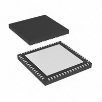
DSPIC33FJ32GS606-I/MR Microchip Technology, DSPIC33FJ32GS606-I/MR Datasheet - Page 191

DSPIC33FJ32GS606-I/MR
Manufacturer Part Number
DSPIC33FJ32GS606-I/MR
Description
16 Bit MCU/DSP 40MIPS 32KB FLASH 64 QFN 9x9x0.9mm TUBE
Manufacturer
Microchip Technology
Series
dsPIC™ 33Fr
Specifications of DSPIC33FJ32GS606-I/MR
Core Processor
dsPIC
Core Size
16-Bit
Speed
40 MIPs
Connectivity
I²C, IrDA, LIN, SPI, UART/USART
Peripherals
Brown-out Detect/Reset, QEI, POR, PWM, WDT
Number Of I /o
58
Program Memory Size
32KB (32K x 8)
Program Memory Type
FLASH
Ram Size
4K x 8
Voltage - Supply (vcc/vdd)
3 V ~ 3.6 V
Data Converters
A/D 16x10b; D/A 1x10b
Oscillator Type
Internal
Operating Temperature
-40°C ~ 85°C
Package / Case
64-VFQFN, Exposed Pad
Lead Free Status / RoHS Status
Lead free / RoHS Compliant
Eeprom Size
-
Lead Free Status / RoHS Status
Lead free / RoHS Compliant
- Current page: 191 of 418
- Download datasheet (3Mb)
FIGURE 9-2:
9.2
The auxiliary clock generation is used for a peripherals
that need to operate at a frequency unrelated to the
system clock such as a PWM or ADC.
The primary oscillator and internal FRC oscillator
sources can be used with an auxiliary PLL to obtain the
auxiliary clock. The auxiliary PLL has a fixed 16x
multiplication factor.
9.3
The reference clock output logic provides the user with
the ability to output a clock signal based on the system
clock or the crystal oscillator on a device pin. The user
application can specify a wide range of clock scaling
prior to outputting the reference clock.
2010 Microchip Technology Inc.
Source (Crystal, External Clock
Note 1: This frequency range must be satisfied at all times.
Note:
Note:
or Internal RC)
dsPIC33FJ32GS406/606/608/610 and dsPIC33FJ64GS406/606/608/610
Auxiliary Clock Generation
Reference Clock Generation
To achieve 1.04 ns PWM resolution, the
auxiliary clock must be set up for 120 MHz.
If the primary PLL is used as a source for
the auxiliary clock, then the primary PLL
should be configured up to a maximum
operation of 30 MIPS or less.
dsPIC33FJ32GS406/606/608/610 and dsPIC33FJ64GS406/606/608/610 PLL
BLOCK DIAGRAM
Divide by
PLLPRE
2-33
N1
0.8-8.0 MHz
Here
Preliminary
(1)
X
Divide by
PLLDIV
2-513
VCO
M
100-200 MHz
Here
F
VCO
(1)
PLLPOST
Divide by
2, 4, 8
N2
12.5-80 MHz
DS70591C-page 191
Here
(1)
F
OSC
Related parts for DSPIC33FJ32GS606-I/MR
Image
Part Number
Description
Manufacturer
Datasheet
Request
R

Part Number:
Description:
IC, DSC, 16BIT, 12KB, 40MHZ, 3.6V, DIP28
Manufacturer:
Microchip Technology
Datasheet:

Part Number:
Description:
Manufacturer:
Microchip Technology Inc.
Datasheet:

Part Number:
Description:
Manufacturer:
Microchip Technology Inc.
Datasheet:

Part Number:
Description:
Manufacturer:
Microchip Technology Inc.
Datasheet:

Part Number:
Description:
Manufacturer:
Microchip Technology Inc.
Datasheet:

Part Number:
Description:
Manufacturer:
Microchip Technology Inc.
Datasheet:

Part Number:
Description:
Manufacturer:
Microchip Technology Inc.
Datasheet:

Part Number:
Description:
Manufacturer:
Microchip Technology Inc.
Datasheet:

Part Number:
Description:
Manufacturer:
Microchip Technology Inc.
Datasheet:


