DSPIC33FJ32GS606-I/MR Microchip Technology, DSPIC33FJ32GS606-I/MR Datasheet - Page 233
DSPIC33FJ32GS606-I/MR
Manufacturer Part Number
DSPIC33FJ32GS606-I/MR
Description
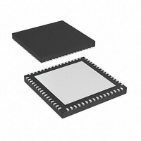
16 Bit MCU/DSP 40MIPS 32KB FLASH 64 QFN 9x9x0.9mm TUBE
Manufacturer
Microchip Technology
Series
dsPIC™ 33Fr
Specifications of DSPIC33FJ32GS606-I/MR
Core Processor
dsPIC
Core Size
16-Bit
Speed
40 MIPs
Connectivity
I²C, IrDA, LIN, SPI, UART/USART
Peripherals
Brown-out Detect/Reset, QEI, POR, PWM, WDT
Number Of I /o
58
Program Memory Size
32KB (32K x 8)
Program Memory Type
FLASH
Ram Size
4K x 8
Voltage - Supply (vcc/vdd)
3 V ~ 3.6 V
Data Converters
A/D 16x10b; D/A 1x10b
Oscillator Type
Internal
Operating Temperature
-40°C ~ 85°C
Package / Case
64-VFQFN, Exposed Pad
Lead Free Status / RoHS Status
Lead free / RoHS Compliant
Eeprom Size
-
Lead Free Status / RoHS Status
Lead free / RoHS Compliant


REGISTER 16-5:
2010 Microchip Technology Inc.
bit 15
bit 7
Legend:
R = Readable bit
-n = Value at POR
bit 15-13
bit 12
bit 11
bit 10
bit 9
bit 8
bit 7
bit 6-4
bit 3-0
dsPIC33FJ32GS406/606/608/610 and dsPIC33FJ64GS406/606/608/610
Note 1: This bit only applies to the secondary master time base period.
SYNCEN
R/W-0
U-0
—
Unimplemented: Read as ‘0’
SESTAT: Special Event Interrupt Status bit
1 = Secondary Special Event Interrupt is pending
0 = Secondary Special Event Interrupt is not pending
SEIEN: Special Event Interrupt Enable bit
1 = Secondary Special Event Interrupt is enabled
0 = Secondary Special Event Interrupt is disabled
EIPU: Enable Immediate Period Updates bit
1 = Active Secondary Period register is updated immediately
0 = Active Secondary Period register updates occur on PWM cycle boundries
SYNCPOL: Synchronize Input and Output Polarity bit
1 = SYNCIx/SYNCO2 polarity is inverted (active-low)
0 = SYNCIx/SYNCO2 polarity is active-high
SYNCOEN: Secondary Master Time Base Sync Enable bit
1 = SYNCO2 output is enabled.
0 = SYNCO2 output is disabled
SYNCEN: External Secondary Master Time Base Synchronization Enable bit
1 = External synchronization of secondary time base is enabled
0 = External synchronization of secondary time base is disabled
SYNCSRC<2:0>: Secondary Time Base Sync Source Selection bits
000 = SYNCI1
001 = SYNCI2
010 = SYNCI3
011 = SYNCI4
100 = Reserved
101 = Reserved
111 = Reserved
SEVTPS<3:0>: PWM Secondary Special Event Trigger Output Postscaler Select bits
1111 = 1:16 Postcale
0001 = 1:2 Postcale
•
•
•
0000 = 1:1 Postscale
R/W-0
U-0
—
STCON: PWM SECONDARY MASTER TIME BASE CONTROL REGISTER
SYNCSRC<2:0>
W = Writable bit
‘1’ = Bit is set
R/W-0
U-0
—
HS/HC-0
SESTAT
R/W-0
Preliminary
U = Unimplemented bit, read as ‘0’
‘0’ = Bit is cleared
(1)
SEIEN
R/W-0
R/W-0
EIPU
R/W-0
R/W-0
SEVTPS<3:0>
(1)
x = Bit is unknown
SYNCPOL
R/W-0
R/W-0
DS70591C-page 233
SYNCOEN
R/W-0
R/W-0
bit 8
bit 0
Related parts for DSPIC33FJ32GS606-I/MR
Image
Part Number
Description
Manufacturer
Datasheet
Request
R

Part Number:
Description:
IC, DSC, 16BIT, 12KB, 40MHZ, 3.6V, DIP28
Manufacturer:
Microchip Technology
Datasheet:

Part Number:
Description:
Manufacturer:
Microchip Technology Inc.
Datasheet:
Part Number:
Description:
Manufacturer:
Microchip Technology Inc.
Datasheet:
Part Number:
Description:
Manufacturer:
Microchip Technology Inc.
Datasheet:
Part Number:
Description:
Manufacturer:
Microchip Technology Inc.
Datasheet:
Part Number:
Description:
Manufacturer:
Microchip Technology Inc.
Datasheet:
Part Number:
Description:
Manufacturer:
Microchip Technology Inc.
Datasheet:
Part Number:
Description:
Manufacturer:
Microchip Technology Inc.
Datasheet:
Part Number:
Description:
Manufacturer:
Microchip Technology Inc.
Datasheet: