CYIL1SM4000AA-GDC Cypress Semiconductor Corp, CYIL1SM4000AA-GDC Datasheet - Page 21
CYIL1SM4000AA-GDC
Manufacturer Part Number
CYIL1SM4000AA-GDC
Description
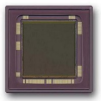
SENSOR IMAGE 4MP CMOS 127-PGA
Manufacturer
Cypress Semiconductor Corp
Type
CMOS Imagingr
Datasheet
1.CYIL1SM4000-EVAL.pdf
(32 pages)
Specifications of CYIL1SM4000AA-GDC
Package / Case
127-PGA
Pixel Size
12µm x 12µm
Active Pixel Array
2048H x 2048V
Frames Per Second
15
Voltage - Supply
2.5V, 3.3V
Operating Supply Voltage
2.5 V
Maximum Operating Temperature
+ 60 C
Minimum Operating Temperature
0 C
Image Size
2048 H x 2048 V
Color Sensing
Monochrome
Package
127CPGA
Operating Temperature
0 to 60 °C
Lead Free Status / RoHS Status
Contains lead / RoHS non-compliant
Lead Free Status / RoHS Status
Lead free / RoHS Compliant, Contains lead / RoHS non-compliant
Other names
LUPA-4000-M
LUPA-4000-M
LUPA-4000-M


Table 10. Pin List
Document Number: 38-05712 Rev. *F
33
34
35
36
37
38
39
40
41
42
43
44
45
46
47
48
49
50
51
52
53
54
55
56
57
58
59
60
61
62
63
64
65
66
67
68
69
70
Pad
L3
Q8
R4
R5
R6
R7
K2
Q9
Q10
R8
R9
R10
R11
Q11
R12
Q12
P15
Q14
Q15
R13
R14
R15
P14
Q13
R16
Q16
P16
N14
N15
L16
L15
N16
M16
L14
M15
K14
J14
M14
Pin
[12, 13, 14]
prebus2
sh_col
pre_col
norowsel
clock_y
sync_y
eos_y_r
temp_diode_p
temp_diode_n
vpix
vmem_l
vmem_h
vres
vres_ds
adc1_ref_low
adc1_linear_conv
adc1_bit_9
adc1_bit_8
adc1_bit_7
adc1_bit_6
adc1_bit_5
adc1_bit_4
adc1_bit_3
adc1_bit_2
adc1_bit_1
adc1_bit_0
adc1_clock
adc1_gndd
adc1_vddd
adc1_gnda
adc1_vdda
adc1_bit_inv
adc1_CMD_SS
adc1_nalog_in
adc1_CMD_FS
adc1_ref_high
vres_ds
vres
Pin Name
(continued)
Input
Input
Input
Input
Input
Input
Testpin
Testpin
Testpin
Supply
Supply
Supply
Supply
Supply
Input
Input
Output
Output
Output
Output
Output
Output
Output
Output
Output
Output
Input
Supply
Supply
Supply
Supply
Input
Input
Input
Input
Supply
Supply
Input
Pin Type
Digital input. Control signal to reduce readout time.
Digital input. Control signal of the column readout.
Digital input. Control signal of the column readout to reduce row-blanking time.
Digital input. Control signal of the column readout.
Digital input. Clock of the Y-addressing.
Digital input. Synchronises the Y-address register.
Indicates when the end of frame is reached when scanning in the 'right'
direction.
Anode of temperature diode.
Cathode of temperature diode.
Power supply pixel array.
Power supply Vmem drivers.
Power supply Vmem drivers.
Power supply reset drivers.
Power supply reset drivers.
Analog reference input. Low reference voltage of ADC (see
resistor value).
Digital input. 1= linear conversion; 0= gamma correction.
Digital output 1 <9> (MSB).
Digital output 1 <8>.
Digital output 1 <7>.
Digital output 1 <6>.
Digital output 1 <5>.
Digital output 1 <4>.
Digital output 1 <3>.
Digital output 1 <2>.
Digital output 1 <1>.
Digital output 1 <0> (LSB).
ADC clock input.
Digital GND of ADC circuitry.
Digital supply of ADC circuitry (nominal 2.5 V).
Analog GND of ADC circuitry.
Analog supply of ADC circuitry (nominal 2.5 V).
Digital input. 0 = no inversion of output bits; 1 = inversion of output bits.
Analog reference input. Biasing of second stage of ADC. Connect to V
R = 50 kΩ and decouple with C = 100 nF to gnda.
Analog input of first ADC.
Analog reference input. Biasing of first stage of ADC. Connect to V
R = 50 kΩand decouple with C = 100 nF to gnda.
Analog reference input. High reference voltage of ADC.
See
Power supply reset drivers.
Power supply reset drivers.
Figure 7
on page 8 for exact resistor value.
Description
CYIL1SM4000AA
Figure 7
Page 21 of 32
DDA
for exact
DDA
with
with
Related parts for CYIL1SM4000AA-GDC
Image
Part Number
Description
Manufacturer
Datasheet
Request
R

Part Number:
Description:
Manufacturer:
Cypress Semiconductor Corp
Datasheet:
Part Number:
Description:
Manufacturer:
Cypress Semiconductor Corp
Datasheet:
Part Number:
Description:
Manufacturer:
Cypress Semiconductor Corp
Datasheet:
Part Number:
Description:
Manufacturer:
Cypress Semiconductor Corp
Datasheet:
Part Number:
Description:
Manufacturer:
Cypress Semiconductor Corp
Datasheet: