CYIL1SM4000AA-GDC Cypress Semiconductor Corp, CYIL1SM4000AA-GDC Datasheet - Page 7
CYIL1SM4000AA-GDC
Manufacturer Part Number
CYIL1SM4000AA-GDC
Description
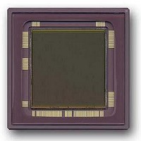
SENSOR IMAGE 4MP CMOS 127-PGA
Manufacturer
Cypress Semiconductor Corp
Type
CMOS Imagingr
Datasheet
1.CYIL1SM4000-EVAL.pdf
(32 pages)
Specifications of CYIL1SM4000AA-GDC
Package / Case
127-PGA
Pixel Size
12µm x 12µm
Active Pixel Array
2048H x 2048V
Frames Per Second
15
Voltage - Supply
2.5V, 3.3V
Operating Supply Voltage
2.5 V
Maximum Operating Temperature
+ 60 C
Minimum Operating Temperature
0 C
Image Size
2048 H x 2048 V
Color Sensing
Monochrome
Package
127CPGA
Operating Temperature
0 to 60 °C
Lead Free Status / RoHS Status
Contains lead / RoHS non-compliant
Lead Free Status / RoHS Status
Lead free / RoHS Compliant, Contains lead / RoHS non-compliant
Other names
LUPA-4000-M
LUPA-4000-M
LUPA-4000-M


Pixel Array Drivers
The image sensor has on-chip drivers for the pixel array signals
The driving on system level is easy and flexible; the maximum
currents applied to the sensor are also controlled on-chip. This
means that the charging on sensor level is fixed; the sensor
cannot be overdriven externally. The operation of the on-chip
drivers is explained in
page 13.
Column Amplifiers
The column amplifiers are designed for minimum power
dissipation and minimum loss of signal, resulting in multiple
biasing signals.
The column amplifiers have an integrated ‘voltage-averaging’
feature. In the voltage-averaging mode, the voltage average
between two columns is read out. In this mode, only 2:1 pixels
must be read out.
To achieve the voltage-averaging mode, an additional external
digital signal called voltage-averaging is required in combination
with a bit from the SPI.
Analog-to-Digital Converter
The LUPA 4000 has two 10-bit flash ADCs running nominally at
10 Msamples/s. The ADC block is electrically separated from the
image sensor. The inputs of the ADC must be tied externally to
the outputs of the output amplifiers. If the internal ADC is not
used, then the power supply pins to the ADC and the I/Os must
be grounded.
Even in this configuration, the internal ADCs are not able to
sustain the 66 Mpixel/sec provided by the output amplifier when
run at full speed.
One ADC samples the even columns and the second ADC
samples the odd columns. Although the input range of the ADC
Note
Document Number: 38-05712 Rev. *F
9. The internal ADC range is typically 50 mV lower than the external applied ADC_VHIGH and ADC_VLOW voltages due to voltage drops over parasitic internal resistors
in the ADC.
Timing and Readout of Image Sensor
100 ns
200 ns
Figure 6. ADC Timing
on
is between 1 V and 2 V and the output range of the analog signal
is between 0.3 V and 1.3 V, the analog output and digital input
may be tied to each other directly. This is possible because there
is an on-chip level-shifter located in front of the ADC to lift up the
analog signal to the ADC range.
Errata for Internal ADCs
Use external ADCs due to the limitation of the internal ADC
clock, not operational at system clock. No fix is intended to
resolve this limitation.
Table 1. ADC Specifications
ADC Timing
The ADC converts the pixel data on the falling edge of the
ADC_CLOCK, but it takes two clock cycles before this pixel data
is at the output of the ADC. This pipeline delay is shown in
Figure
Input range
Quantization
Nominal data rate
Differential nonlinearity (DNL) -
linear conversion mode
Integral nonlinearity (INL) -
linear conversion mode
Input capacitance
Power dissipation at 33 MHz
Conversion law
6.
Parameter
10 bits
Linear/Gamma-corrected
1 V to 2 V
10 Msamples/s
Typ < 0.4 LSB RMS
Typ < 3.5 LSB
< 2 pF
50 mW
CYIL1SM4000AA
Specification
[9]
Page 7 of 32
Related parts for CYIL1SM4000AA-GDC
Image
Part Number
Description
Manufacturer
Datasheet
Request
R

Part Number:
Description:
Manufacturer:
Cypress Semiconductor Corp
Datasheet:
Part Number:
Description:
Manufacturer:
Cypress Semiconductor Corp
Datasheet:
Part Number:
Description:
Manufacturer:
Cypress Semiconductor Corp
Datasheet:
Part Number:
Description:
Manufacturer:
Cypress Semiconductor Corp
Datasheet:
Part Number:
Description:
Manufacturer:
Cypress Semiconductor Corp
Datasheet: