CYIL1SM4000AA-GDC Cypress Semiconductor Corp, CYIL1SM4000AA-GDC Datasheet - Page 6
CYIL1SM4000AA-GDC
Manufacturer Part Number
CYIL1SM4000AA-GDC
Description
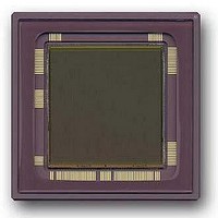
SENSOR IMAGE 4MP CMOS 127-PGA
Manufacturer
Cypress Semiconductor Corp
Type
CMOS Imagingr
Datasheet
1.CYIL1SM4000-EVAL.pdf
(32 pages)
Specifications of CYIL1SM4000AA-GDC
Package / Case
127-PGA
Pixel Size
12µm x 12µm
Active Pixel Array
2048H x 2048V
Frames Per Second
15
Voltage - Supply
2.5V, 3.3V
Operating Supply Voltage
2.5 V
Maximum Operating Temperature
+ 60 C
Minimum Operating Temperature
0 C
Image Size
2048 H x 2048 V
Color Sensing
Monochrome
Package
127CPGA
Operating Temperature
0 to 60 °C
Lead Free Status / RoHS Status
Contains lead / RoHS non-compliant
Lead Free Status / RoHS Status
Lead free / RoHS Compliant, Contains lead / RoHS non-compliant
Other names
LUPA-4000-M
LUPA-4000-M
LUPA-4000-M


Sensor Architecture
The LUPA 4000 architecture is shown in
Image Core
The image core consists of a pixel array, one X-addressing and
two Y-addressing registers (only one drawn), pixel array drivers,
and column amplifiers.
The active pixel area is read out in progressive scan by one or
two output amplifiers. The output amplifiers operate at a nomimal
Output Amplifier
The sensor has two output amplifiers. A single amplifier can be
operated at 66 Mpixels/sec to bring the whole pixel array of 2048
by 2048 pixels at the required frame rate. The second output
amplifier can be enabled in parallel if the clock frequency is
decreased to 33 Msamples/sec. Using only one output-stage,
the output signal is the result of multiplexing between the two
internal buses. When using two output-stages, both outputs are
in phase.
Each output-stage has two outputs. One output is the pixel
signal; the second output is a DC signal, which offset can be
programmed using a 7-bit word. The DC signal is used for
common mode rejection between the two signals. The
disadvantage is an increase in power dissipation. However, this
can be reduced by setting the highest DAC voltage using the
SPI.
Document Number: 38-05712 Rev. *F
Clk_y Sync_y
Eos_y
Figure
Figure 4. Block Diagram of Image Sensor
(reset, mem_hl, precharge, sample)
Clk_x Sync_x
4.
Pixel
(0,0)
Blocks
Logic
On-chip drivers
Column Amplifiers
X-shift registers
(2048 x 2048)
Pixel Array
SPI
speed of 66-MHz pixel rate, or 33-MHz pixel rate if two output
amplifiers are used to read out the imager. The image sensor is
designed for operation up to 66 MHz.
The structure allows having a programmable addressing in the
x-direction and y-direction in steps of two. Only even start
addresses in x-direction and y-direction are possible. The
starting point of the address can be uploaded using the SPI.
Figure 5. Output Stage Architecture.
The output voltage of Output1 is between 1.3 V (dark level) and
0.3 V (white level) and depends on process variations and
voltage supply settings. The output voltage of Output2 is
determined by the DAC.
2 Differential Outputs
SPI
Image Sensor
DAC
7 bits
DAC
Eos_x
CYIL1SM4000AA
(Pixel Signal)
(dc signal)
Output 1
Output 2
Page 6 of 32
Related parts for CYIL1SM4000AA-GDC
Image
Part Number
Description
Manufacturer
Datasheet
Request
R

Part Number:
Description:
Manufacturer:
Cypress Semiconductor Corp
Datasheet:
Part Number:
Description:
Manufacturer:
Cypress Semiconductor Corp
Datasheet:
Part Number:
Description:
Manufacturer:
Cypress Semiconductor Corp
Datasheet:
Part Number:
Description:
Manufacturer:
Cypress Semiconductor Corp
Datasheet:
Part Number:
Description:
Manufacturer:
Cypress Semiconductor Corp
Datasheet: