STGW30N90D STMicroelectronics, STGW30N90D Datasheet
STGW30N90D
Specifications of STGW30N90D
STGW30N90D
Available stocks


Related parts for STGW30N90D


STGW30N90D Summary of contents
Page 1
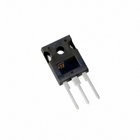
... Table 1. Device summary Order code STGW30N90D September 2009 ) Figure 1. Marking Package GW30N90D TO-247 Doc ID 13766 Rev 2 STGW30N90D 30 A, 900 V very fast IGBT TO-247 Internal schematic diagram Packaging Tube 1/13 www.st.com 13 ...
Page 2
... Contents Contents 1 Electrical ratings . . . . . . . . . . . . . . . . . . . . . . . . . . . . . . . . . . . . . . . . . . . . 3 2 Electrical characteristics . . . . . . . . . . . . . . . . . . . . . . . . . . . . . . . . . . . . . 4 2.1 Electrical characteristics (curves) 3 Test circuit . . . . . . . . . . . . . . . . . . . . . . . . . . . . . . . . . . . . . . . . . . . . . . . . 9 4 Package mechanical data . . . . . . . . . . . . . . . . . . . . . . . . . . . . . . . . . . . . 10 5 Revision history . . . . . . . . . . . . . . . . . . . . . . . . . . . . . . . . . . . . . . . . . . . 12 2/ Doc ID 13766 Rev 2 STGW30N90D ...
Page 3
... STGW30N90D 1 Electrical ratings Table 2. Absolute maximum ratings Symbol V Collector-emitter voltage (V CES (1) I Collector current (continuous (1) I Collector current (continuous (2) I Turn-off latching current CL (3) I Pulsed collector current CP V Gate-emitter voltage GE P Total dissipation at T TOT I Diode RMS forward current Surge non repetitive forward current t ...
Page 4
... Test conditions 600 600 =± Parameter Test conditions MHz 900 A Doc ID 13766 Rev 2 STGW30N90D Min. Typ. 900 = =125 °C 2 250µA 3.75 =125 ° Min. Typ. 2510 =0 - 175 GE 30 110 - 16 = Max. Unit V 2. 5.75 V 500 µ ± 100 nA S Max. Unit ...
Page 5
... STGW30N90D Table 6. Switching on/off (inductive load) Symbol t Turn-on delay time d(on) t Current rise time r (di/dt) Turn-on current slope on t Turn-on delay time d(on) t Current rise time r (di/dt) Turn-on current slope Off voltage rise time r off Turn-off delay time d off t Current fall time ...
Page 6
... Electrical characteristics 2.1 Electrical characteristics (curves) Figure 2. Output characteristics Figure 4. Transconductance Figure 6. Gate charge vs. gate-source voltage Figure 7. 6/13 Figure 3. Transfer characteristics Figure 5. Collector-emitter on voltage vs. temperature Capacitance variations Doc ID 13766 Rev 2 STGW30N90D ...
Page 7
... STGW30N90D Figure 8. Normalized gate threshold voltage vs. temperature Figure 10. Normalized breakdown voltage vs. temperature Figure 12. Switching losses vs. gate resistance Figure 9. Collector-emitter on voltage vs. collector current Figure 11. Switching losses vs. temperature Figure 13. Switching losses vs. collector current Doc ID 13766 Rev 2 Electrical characteristics 7/13 ...
Page 8
... Figure 14. Thermal Impedance Figure 16. Forward voltage drop vs. forward current I (A) FM 100 90 T =150˚C j (typical values =150˚ (maximum values 0.0 0.5 1.0 1.5 2.0 2.5 8/13 Figure 15. Reverse biased SOA T =25˚C j (maximum values) (V) 3.0 3.5 4.0 4.5 Doc ID 13766 Rev 2 STGW30N90D ...
Page 9
... STGW30N90D 3 Test circuit Figure 17. Test circuit for inductive load switching Figure 19. Switching waveform Td(off) Td(on) Tr(Ion) Ton Figure 18. Gate charge test circuit AM01504v1 Figure 20. Diode recovery time waveform 90% 10 90% 10% Tr(Voff) Tcross 90% 10% Tf Toff AM01506v1 Doc ID 13766 Rev 2 Test circuit Q di/dt ...
Page 10
... Package mechanical data 4 Package mechanical data In order to meet environmental requirements, ST offers these devices in different grades of ® ECOPACK packages, depending on their level of environmental compliance. ECOPACK specifications, grade definitions and product status are available at: www.st.com. ECOPACK trademark. 10/13 Doc ID 13766 Rev 2 STGW30N90D ® ...
Page 11
... STGW30N90D Dim øP øR S TO-247 mechanical data mm. Min. Typ. 4.85 2.20 1.0 2.0 3.0 0.40 19.85 15.45 5.45 14.20 3.70 18.50 3.55 4.50 5.50 Doc ID 13766 Rev 2 Package mechanical data Max. 5.15 2.60 1.40 2.40 3.40 0.80 20.15 15.75 14.80 4.30 3 ...
Page 12
... Revision history 5 Revision history Table 9. Document revision history Date 19-Jul-2006 02-Sep-2009 12/13 Revision 1 First issue. – Document status promoted from preliminary data to datasheet 2 Section 4: Package mechanical data – Doc ID 13766 Rev 2 STGW30N90D Changes has been updated ...
Page 13
... STGW30N90D Information in this document is provided solely in connection with ST products. STMicroelectronics NV and its subsidiaries (“ST”) reserve the right to make changes, corrections, modifications or improvements, to this document, and the products and services described herein at any time, without notice. All ST products are sold pursuant to ST’s terms and conditions of sale. ...