STGW40NC60V STMicroelectronics, STGW40NC60V Datasheet - Page 3
STGW40NC60V
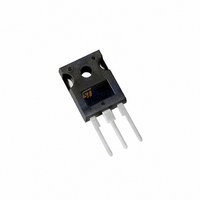
Manufacturer Part Number
STGW40NC60V
Description
IGBT N-CHAN 80A 600V TO247
Manufacturer
STMicroelectronics
Series
PowerMESH™r
Datasheet
1.STGW40NC60V.pdf
(10 pages)
Specifications of STGW40NC60V
Voltage - Collector Emitter Breakdown (max)
600V
Vce(on) (max) @ Vge, Ic
2.5V @ 15V, 40A
Current - Collector (ic) (max)
80A
Power - Max
260W
Input Type
Standard
Mounting Type
Through Hole
Package / Case
TO-247-3
Transistor Type
IGBT
Dc Collector Current
80A
Collector Emitter Voltage Vces
2.5V
Power Dissipation Pd
260W
Collector Emitter Voltage V(br)ceo
600V
Transistor Case Style
TO-247
No. Of Pins
3
Svhc
No
Rohs Compliant
Yes
Operating Temperature Range
-55°C To +150°C
Lead Free Status / RoHS Status
Lead free / RoHS Compliant
Igbt Type
-
Other names
497-4358-5
Available stocks
Company
Part Number
Manufacturer
Quantity
Price
Company:

Part Number:
STGW40NC60V
Manufacturer:
ST
Quantity:
12 500


ELECTRICAL CHARACTERISTICS (CONTINUED)
Table 7: Dynamic
Table 8: Switching On
2) Eon is the turn-on losses when a typical diode is used in the test circuit in figure 2. If the IGBT is offered in a package with a co-pack diode,
the co-pack diode is used as external diode. IGBTs & DIODE are at the same temperature (25°C and 125°C)
Table 9: Switching Off
(3)Turn-off losses include also the tail of the collector current.
Symbol
Symbol
Symbol
(di/dt)
(di/dt)
Eon (2)
Eon (2)
E
E
t
t
g
t
t
t
t
r
r
C
C
C
Q
d
d
Q
d(on)
d(on)
(V
off
(V
off
fs
I
E
E
Q
CL
(
(
oes
t
t
res
t
t
ies
(1)
ge
gc
off
off
r
r
f
ts
f
ts
g
off
off
(3)
(3)
on
on
)
)
)
)
Forward Transconductance
Input Capacitance
Output Capacitance
Reverse Transfer
Capacitance
Total Gate Charge
Gate-Emitter Charge
Gate-Collector Charge
Turn-Off SOA Minimum
Current
Turn-on Delay Time
Current Rise Time
Turn-on Current Slope
Turn-on Switching Losses
Turn-on Delay Time
Current Rise Time
Turn-on Current Slope
Turn-on Switching Losses
Off Voltage Rise Time
Turn-off Delay Time
Current Fall Time
Turn-off Switching Loss
Total Switching Loss
Off Voltage Rise Time
Turn-off Delay Time
Current Fall Time
Turn-off Switching Loss
Total Switching Loss
Parameter
Parameter
Parameter
V
V
V
V
(see Figure 20)
V
R
V
R
(see Figure 18)
V
R
125°C
(see Figure 18)
V
R
T
(see Figure 18)
V
R
Tj = 125 °C
(see Figure 18)
CE
CE
CE
GE
clamp
CC
CC
J
G
G
G
cc
cc
GE
GE
= 3.3 , V
= 3.3 , V
= 25 °C
= 100
= 390 V, I
= 390 V, I
= 15 V
= 25V, f = 1 MHz, V
= 390 V, I
= 15V,
= 390 V, I
= 390 V, I
= 3.3
= 3.3
= 480 V Tj = 150°C
Test Conditions
Test Conditions
Test Conditions
,
I
GE
GE
C
V
, V
, V
C
C
= 20 A
C
GE
C
C
= 15V, Tj= 25°C
= 15V, Tj=
= 40 A,
= 40 A,
GE
GE
= 40 A,
= 40 A
= 40 A
= 15V
= 15 V
= 15 V
GE
= 0
Min.
Min.
Min.
200
4550
2060
1900
Typ.
Typ.
1050
1400
2040
350
105
214
330
640
Typ.
140
720
170
20
30
96
43
17
42
19
25
45
60
77
STGW40NC60V
Max.
Max.
Max.
1420
450
970
A/µs
A/µs
Unit
Unit
Unit
nC
nC
nC
pF
pF
pF
µJ
µJ
ns
ns
ns
ns
ns
ns
ns
ns
ns
ns
3/10
S
A
J
J
J
J
Related parts for STGW40NC60V
Image
Part Number
Description
Manufacturer
Datasheet
Request
R

Part Number:
Description:
STMicroelectronics [RIPPLE-CARRY BINARY COUNTER/DIVIDERS]
Manufacturer:
STMicroelectronics
Datasheet:
Part Number:
Description:
STMicroelectronics [LIQUID-CRYSTAL DISPLAY DRIVERS]
Manufacturer:
STMicroelectronics
Datasheet:

Part Number:
Description:
BOARD EVAL FOR MEMS SENSORS
Manufacturer:
STMicroelectronics
Datasheet:
Part Number:
Description:
NPN TRANSISTOR POWER MODULE
Manufacturer:
STMicroelectronics
Datasheet:
Part Number:
Description:
TURBOSWITCH ULTRA-FAST HIGH VOLTAGE DIODE
Manufacturer:
STMicroelectronics
Datasheet:
Part Number:
Description:
Manufacturer:
STMicroelectronics
Datasheet:
Part Number:
Description:
DIODE / SCR MODULE
Manufacturer:
STMicroelectronics
Datasheet:
Part Number:
Description:
DIODE / SCR MODULE
Manufacturer:
STMicroelectronics
Datasheet:
Part Number:
Description:
Search -----> STE16N100
Manufacturer:
STMicroelectronics
Datasheet:
Part Number:
Description:
Search ---> STE53NA50
Manufacturer:
STMicroelectronics
Datasheet:
Part Number:
Description:
NPN Transistor Power Module
Manufacturer:
STMicroelectronics
Datasheet:
Part Number:
Description:
DIODE / SCR MODULE
Manufacturer:
STMicroelectronics
Datasheet: