IXGH17N100AU1 IXYS, IXGH17N100AU1 Datasheet - Page 2
IXGH17N100AU1
Manufacturer Part Number
IXGH17N100AU1
Description
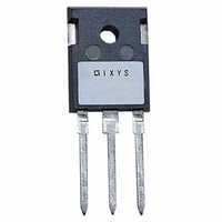
IGBT LOW VOLT 1000V 34A TO-247AD
Manufacturer
IXYS
Series
HiPerFAST™r
Datasheet
1.IXGH17N100AU1.pdf
(6 pages)
Specifications of IXGH17N100AU1
Voltage - Collector Emitter Breakdown (max)
1000V
Vce(on) (max) @ Vge, Ic
4V @ 15V, 17A
Current - Collector (ic) (max)
34A
Power - Max
150W
Input Type
Standard
Mounting Type
Through Hole
Package / Case
TO-247AD
Channel Type
N
Configuration
Single
Collector-emitter Voltage
1kV
Gate To Emitter Voltage (max)
±20V
Package Type
TO-247AD
Pin Count
3
Mounting
Through Hole
Operating Temperature (max)
150C
Operating Temperature Classification
Military
Vces, (v)
1000
Ic25, Tc=25°c, Igbt, (a)
34
Ic90, Tc=90°c, Igbt, (a)
17
Ic110, Tc=110°c, Igbt, (a)
-
Vce(sat), Max, Tj=25°c, Igbt, (v)
4
Tfi, Typ, Tj=25°c, Igbt, (ns)
450
Eoff, Typ, Tj=125°c, Igbt, (mj)
6
Rthjc, Max, Igbt, (°c/w)
0.83
If, Tj=110°c, Diode, (a)
17
Rthjc, Max, Diode, (ºc/w)
1.0
Package Style
TO-247
Lead Free Status / RoHS Status
Lead free / RoHS Compliant
Igbt Type
-
Lead Free Status / RoHS Status
Compliant, Lead free / RoHS Compliant
Available stocks
Company
Part Number
Manufacturer
Quantity
Price
Company:

Part Number:
IXGH17N100AU1
Manufacturer:
IXYS
Quantity:
15 500


IXYS reserves the right to change limits, test conditions, and dimensions.
IXYS MOSFETS and IGBTs are covered by one or more of the following U.S. patents:
Symbol
g
C
C
C
Q
Q
Q
t
t
t
t
E
t
t
E
t
t
E
R
R
Reverse Diode (FRED)
Symbol
V
I
t
R
ri
fi
ri
fi
rr
d(on)
d(off)
d(on)
d(off)
RM
fs
off
on
off
ies
oes
res
thJC
thCK
F
thJC
g
ge
gc
Test Conditions
I
Pulse test, t
V
I
Test Conditions
I
Pulse test, t
I
V
I
Inductive load, T
I
V
Remarks: Switching times
may increase
for V
higher T
Inductive load, T
I
V
Remarks: Switching times
may increase
for V
higher T
C
F
F
F
C
C
C
CE
R
CE
CE
= I
= I
= 1 A; -di/dt = 100 A/ s; V
= I
= I
= I
= 540 V
= 25 V, V
= 0.8 V
= 0.8 V
= I
C90
C90
C90
C90
CE
C90
CE
, V
, V
C90
, V
, V
, V
(Clamp) > 0.8 • V
(Clamp) > 0.8 • V
J
J
; V
GE
GE
GE
or increased R
or increased R
GE
GE
CES
CES
= 0 V,
= 0 V, -di
CE
= 15 V, V
= 15 V, L = 300 H,
= 15 V, L = 300 H
GE
, R
, R
300 s, duty cycle
300 s, duty cycle d
= 10 V,
= 0 V, f = 1 MHz
G
G
J
J
= R
= R
= 25 C
= 125 C
F
CE
off
off
/dt = 240 A/ s
= 82
= 82
= 0.5 V
G
G
CES
CES
,
,
R
(T
(T
= 30 V T
J
J
CES
= 25 C, unless otherwise specified)
= 25 C, unless otherwise specified)
2 %
17N100U1
17N100AU1
17N100AU1
17N100U1
17N100AU1
17N100U1
17N100AU1
2 %
T
J
J
= 125 C
= 25 C
min.
min.
Characteristic Values
Characteristic Values
6
1500
1200
typ.
0.25
typ.
120
210
100
100
200
500
750
450
100
200
700
750
2.5
16
35
4,835,592
4,850,072
15
40
20
60
3
8
6
max.
max.
1000
1000
2000
1000
0.83 K/W
120
750
2.5
18
50
30
90
1 K/W
4,881,106
4,931,844
K/W
mJ
mJ
nC
nC
nC
mJ
mJ
pF
pF
pF
ns
ns
ns
ns
ns
ns
ns
ns
ns
ns
ns
ns
S
V
A
5,017,508
5,034,796
TO-247 AD Outline
1 = Gate
2 = Collector
3 = Emitter
Tab = Collector
IXGH 17N100U1
IXGH 17N100AU1
5,049,961
5,063,307
5,187,117
5,237,481
5,486,715
5,381,025
Related parts for IXGH17N100AU1
Image
Part Number
Description
Manufacturer
Datasheet
Request
R


Part Number:
Description:
HiPerFET Power MOSFETs
Manufacturer:
IXYS Corporation
Datasheet:
Part Number:
Description:
J-K-Type Flip-Flop
Manufacturer:
IXYS Corporation
Datasheet:
Part Number:
Description:
HiPerRF Power MOSFETs
Manufacturer:
IXYS Corporation
Datasheet:
Part Number:
Description:
Rectifier Module for Three Phase Power Factor Correction
Manufacturer:
IXYS Corporation
Datasheet:
Part Number:
Description:
Thyristor Modules Thyristor/Diode Modules
Manufacturer:
IXYS Corporation
Datasheet:
Part Number:
Description:
Thyristor Modules Thyristor/Diode Modules
Manufacturer:
IXYS Corporation
Datasheet:
Part Number:
Description:
Thyristor Modules Thyristor/Diode Modules
Manufacturer:
IXYS Corporation
Datasheet:
Part Number:
Description:
Thyristor Modules Thyristor/Diode Modules
Manufacturer:
IXYS Corporation
Datasheet:
Part Number:
Description:
Thyristor Modules /Diode Modules
Manufacturer:
IXYS Corporation
Datasheet:
Part Number:
Description:
Thyristor Modules /Diode Modules
Manufacturer:
IXYS Corporation
Datasheet:
Part Number:
Description:
Thyristor Modules Thyristor/Diode Modules
Manufacturer:
IXYS Corporation
Datasheet: