NTHD4508NT1G ON Semiconductor, NTHD4508NT1G Datasheet - Page 2
NTHD4508NT1G
Manufacturer Part Number
NTHD4508NT1G
Description
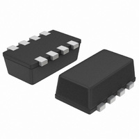
MOSFET 2N-CH 20V 3.1A CHIPFET
Manufacturer
ON Semiconductor
Datasheet
1.NTHD4508NT1G.pdf
(6 pages)
Specifications of NTHD4508NT1G
Fet Type
2 N-Channel (Dual)
Fet Feature
Logic Level Gate
Rds On (max) @ Id, Vgs
75 mOhm @ 3.1A, 4.5V
Drain To Source Voltage (vdss)
20V
Current - Continuous Drain (id) @ 25° C
3A
Vgs(th) (max) @ Id
1.2V @ 250µA
Gate Charge (qg) @ Vgs
4nC @ 4.5V
Input Capacitance (ciss) @ Vds
180pF @ 10V
Power - Max
1.13W
Mounting Type
Surface Mount
Package / Case
8-ChipFET™
Configuration
Dual Dual Drain
Transistor Polarity
N-Channel
Resistance Drain-source Rds (on)
0.075 Ohm @ 4.5 V
Forward Transconductance Gfs (max / Min)
6 S
Drain-source Breakdown Voltage
20 V
Gate-source Breakdown Voltage
+/- 12 V
Continuous Drain Current
3 A
Power Dissipation
1130 mW
Maximum Operating Temperature
+ 150 C
Mounting Style
SMD/SMT
Minimum Operating Temperature
- 55 C
Lead Free Status / RoHS Status
Lead free / RoHS Compliant
Other names
NTHD4508NT1GOSTR
Available stocks
Company
Part Number
Manufacturer
Quantity
Price
Company:

Part Number:
NTHD4508NT1G
Manufacturer:
ON Semiconductor
Quantity:
35 997
Part Number:
NTHD4508NT1G
Manufacturer:
ON/安森美
Quantity:
20 000


2. Pulse Test: Pulse Width v 300 ms, Duty Cycle v 2%.
3. Switching characteristics are independent of operating junction temperatures.
ELECTRICAL CHARACTERISTICS
OFF CHARACTERISTICS
ON CHARACTERISTICS (Note 2)
CHARGES AND CAPACITANCES
SWITCHING CHARACTERISTICS (Note 3)
DRAIN−SOURCE DIODE CHARACTERISTICS
Drain−to−Source Breakdown Voltage
Zero Gate Voltage Drain Current
Gate−to−Source Leakage Current
Gate Threshold Voltage
Drain−to−Source On−Resistance
Forward Transconductance
Input Capacitance
Output Capacitance
Reverse Transfer Capacitance
Total Gate Charge
Threshold Gate Charge
Gate−to−Source Charge
Gate−to−Drain Charge
Turn−On Delay Time
Rise Time
Turn−Off Delay Time
Fall Time
Forward Diode Voltage
Reverse Recovery Time
Charge Time
Discharge Time
Reverse Recovery Charge
Parameter
(T
J
= 25 C unless otherwise noted)
V
Symbol
V
Q
R
Q
t
(BR)DSS
C
C
t
d(OFF)
GS(TH)
I
I
C
G(TOT)
Q
Q
Q
DS(on)
d(ON)
V
g
DSS
GSS
G(TH)
t
OSS
RSS
RR
ta
tb
FS
ISS
t
t
SD
GS
GD
RR
r
f
(
)
http://onsemi.com
NTHD4508N
V
GS
V
V
V
V
= 0 V, V
V
V
V
V
V
GS
GS
GS
GS
V
I
V
V
DS
GS
D
GS
V
V
V
2
GS
DS
GS
GS
GS
GS
GS
= 3.1 A, R
dI
Test Conditions
= 4.5 V, V
= 4.5 V, V
= 4.5 V, V
= 4.5 V, V
= 0 V, V
= 0 V, f = 1.0 MHz,
= V
S
= 0 V, V
= 10 V, I
= 0 V, I
= 0 V, I
= 4.5, I
= 2.5, I
V
V
= 0 V, I
/dt = 100 A/ms
0 V f
V
I
DS
D
DS
DS
GS
DS
= 3.1 A
= 16 V, T
, I
= 10 V
= 10 V
= 0 V
GS
D
S
S
D
D
S
DS
G
DS
DS
DS
DS
D
1 0 MH
= 1.5 A,
= 1.5 A,
= 250 mA
= 3.1 A
= 2.3 A
= 3.1 A
= "12 V
= 2.5 W
= 3.1 A
= 16 V
= 10 V,
= 10 V,
= 16 V,
= 16 V,
J
= 125 C
Min
0.6
20
0.75
12.5
Typ
180
6.0
2.6
0.5
0.6
0.7
5.0
3.0
9.0
3.5
6.0
60
80
80
25
15
10
"100
Max
1.15
115
1.0
1.2
4.0
6.0
10
75
10
30
20
Units
mW
mA
nA
pF
nC
nC
ns
ns
V
V
S
V
Related parts for NTHD4508NT1G
Image
Part Number
Description
Manufacturer
Datasheet
Request
R

Part Number:
Description:
ON Semiconductor [VOLTAGE REGULATOR]
Manufacturer:
ON Semiconductor
Datasheet:
Part Number:
Description:
357-036-542-201 CARDEDGE 36POS DL .156 BLK LOPRO
Manufacturer:
ON Semiconductor
Datasheet:
Part Number:
Description:
357-036-542-201 CARDEDGE 36POS DL .156 BLK LOPRO
Manufacturer:
ON Semiconductor
Datasheet:
Part Number:
Description:
357-036-542-201 CARDEDGE 36POS DL .156 BLK LOPRO
Manufacturer:
ON Semiconductor
Datasheet:
Part Number:
Description:
357-036-542-201 CARDEDGE 36POS DL .156 BLK LOPRO
Manufacturer:
ON Semiconductor
Datasheet:
Part Number:
Description:
357-036-542-201 CARDEDGE 36POS DL .156 BLK LOPRO
Manufacturer:
ON Semiconductor
Datasheet:
Part Number:
Description:
357-036-542-201 CARDEDGE 36POS DL .156 BLK LOPRO
Manufacturer:
ON Semiconductor
Datasheet:
Part Number:
Description:
357-036-542-201 CARDEDGE 36POS DL .156 BLK LOPRO
Manufacturer:
ON Semiconductor
Datasheet:
Part Number:
Description:
357-036-542-201 CARDEDGE 36POS DL .156 BLK LOPRO
Manufacturer:
ON Semiconductor
Datasheet:
Part Number:
Description:
357-036-542-201 CARDEDGE 36POS DL .156 BLK LOPRO
Manufacturer:
ON Semiconductor
Datasheet:
Part Number:
Description:
357-036-542-201 CARDEDGE 36POS DL .156 BLK LOPRO
Manufacturer:
ON Semiconductor
Datasheet:
Part Number:
Description:
Manufacturer:
ON Semiconductor
Datasheet:
Part Number:
Description:
Manufacturer:
ON Semiconductor
Datasheet:
Part Number:
Description:
Manufacturer:
ON Semiconductor
Datasheet: