NTHD4508NT1G ON Semiconductor, NTHD4508NT1G Datasheet - Page 5
NTHD4508NT1G
Manufacturer Part Number
NTHD4508NT1G
Description
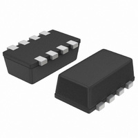
MOSFET 2N-CH 20V 3.1A CHIPFET
Manufacturer
ON Semiconductor
Datasheet
1.NTHD4508NT1G.pdf
(6 pages)
Specifications of NTHD4508NT1G
Fet Type
2 N-Channel (Dual)
Fet Feature
Logic Level Gate
Rds On (max) @ Id, Vgs
75 mOhm @ 3.1A, 4.5V
Drain To Source Voltage (vdss)
20V
Current - Continuous Drain (id) @ 25° C
3A
Vgs(th) (max) @ Id
1.2V @ 250µA
Gate Charge (qg) @ Vgs
4nC @ 4.5V
Input Capacitance (ciss) @ Vds
180pF @ 10V
Power - Max
1.13W
Mounting Type
Surface Mount
Package / Case
8-ChipFET™
Configuration
Dual Dual Drain
Transistor Polarity
N-Channel
Resistance Drain-source Rds (on)
0.075 Ohm @ 4.5 V
Forward Transconductance Gfs (max / Min)
6 S
Drain-source Breakdown Voltage
20 V
Gate-source Breakdown Voltage
+/- 12 V
Continuous Drain Current
3 A
Power Dissipation
1130 mW
Maximum Operating Temperature
+ 150 C
Mounting Style
SMD/SMT
Minimum Operating Temperature
- 55 C
Lead Free Status / RoHS Status
Lead free / RoHS Compliant
Other names
NTHD4508NT1GOSTR
Available stocks
Company
Part Number
Manufacturer
Quantity
Price
Company:

Part Number:
NTHD4508NT1G
Manufacturer:
ON Semiconductor
Quantity:
35 997
Part Number:
NTHD4508NT1G
Manufacturer:
ON/安森美
Quantity:
20 000


Figure 11. This is sufficient for low power dissipation
MOSFET
performance requires a greater copper pad area, particularly
for the drain leads.
12 improves the thermal area of the drain connections (pins
5, 6, 7, 8) while remaining within the confines of the basic
The basic pad layout with dimensions is shown in
The minimum recommended pad pattern shown in Figure
0.457
0.018
applications,
0.026
0.66
Figure 11. Basic
2.032
0.08
0.711
0.028
but
*For additional information on our Pb−Free strategy and soldering
details, please download the ON Semiconductor Soldering and
Mounting Techniques Reference Manual, SOLDERRM/D.
power
semiconductor
SOLDERING FOOTPRINTS*
BASIC PAD PATTERNS
0.635
0.025
http://onsemi.com
NTHD4508N
5
footprint. The drain copper area is 0.0019 sq. in. (or 1.22 sq.
mm). This will assist the power dissipation path away from
the device (through the copper lead−frame) and into the
board and exterior chassis (if applicable) for the single
device. The addition of a further copper area and/or the
addition of vias to other board layers will enhance the
performance still further.
0.457
0.018
0.635
0.025
0.026
0.66
Figure 12. Style 2
2.032
0.08
0.254
0.010
SCALE 20:1
1.032
0.043
inches
mm
0.178
0.007
Related parts for NTHD4508NT1G
Image
Part Number
Description
Manufacturer
Datasheet
Request
R

Part Number:
Description:
ON Semiconductor [VOLTAGE REGULATOR]
Manufacturer:
ON Semiconductor
Datasheet:
Part Number:
Description:
357-036-542-201 CARDEDGE 36POS DL .156 BLK LOPRO
Manufacturer:
ON Semiconductor
Datasheet:
Part Number:
Description:
357-036-542-201 CARDEDGE 36POS DL .156 BLK LOPRO
Manufacturer:
ON Semiconductor
Datasheet:
Part Number:
Description:
357-036-542-201 CARDEDGE 36POS DL .156 BLK LOPRO
Manufacturer:
ON Semiconductor
Datasheet:
Part Number:
Description:
357-036-542-201 CARDEDGE 36POS DL .156 BLK LOPRO
Manufacturer:
ON Semiconductor
Datasheet:
Part Number:
Description:
357-036-542-201 CARDEDGE 36POS DL .156 BLK LOPRO
Manufacturer:
ON Semiconductor
Datasheet:
Part Number:
Description:
357-036-542-201 CARDEDGE 36POS DL .156 BLK LOPRO
Manufacturer:
ON Semiconductor
Datasheet:
Part Number:
Description:
357-036-542-201 CARDEDGE 36POS DL .156 BLK LOPRO
Manufacturer:
ON Semiconductor
Datasheet:
Part Number:
Description:
357-036-542-201 CARDEDGE 36POS DL .156 BLK LOPRO
Manufacturer:
ON Semiconductor
Datasheet:
Part Number:
Description:
357-036-542-201 CARDEDGE 36POS DL .156 BLK LOPRO
Manufacturer:
ON Semiconductor
Datasheet:
Part Number:
Description:
357-036-542-201 CARDEDGE 36POS DL .156 BLK LOPRO
Manufacturer:
ON Semiconductor
Datasheet:
Part Number:
Description:
Manufacturer:
ON Semiconductor
Datasheet:
Part Number:
Description:
Manufacturer:
ON Semiconductor
Datasheet:
Part Number:
Description:
Manufacturer:
ON Semiconductor
Datasheet: