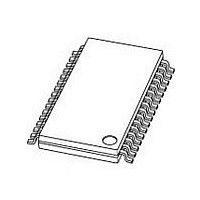
TDA8932BTW NXP Semiconductors, TDA8932BTW Datasheet - Page 27

TDA8932BTW
Manufacturer Part Number
TDA8932BTW
Description
Audio Amplifiers 2X15W BTL CLASS D AMP+VOLCTRL
Manufacturer
NXP Semiconductors
Datasheet
1.TDA8932BTW.pdf
(48 pages)
Specifications of TDA8932BTW
Product
Class-D
Output Power
55 W
Available Set Gain
36 dB
Common Mode Rejection Ratio (min)
75 dB
Thd Plus Noise
0.007 %
Operating Supply Voltage
22 V
Supply Current
0.6 mA
Maximum Power Dissipation
5000 mW
Maximum Operating Temperature
+ 85 C
Mounting Style
SMD/SMT
Audio Load Resistance
8 Ohms
Dual Supply Voltage
+/- 11 V
Input Signal Type
Differential
Minimum Operating Temperature
- 40 C
Output Signal Type
Differential, Single
Supply Type
Single or Dual
Supply Voltage (max)
36 V
Supply Voltage (min)
10 V
Output Type
1-Channel Mono or 2-Channel Stereo
Package / Case
HTSSOP-32
Operational Class
Class-D
Audio Amplifier Output Configuration
1-Channel Mono/2-Channel Stereo
Audio Amplifier Function
Speaker
Total Harmonic Distortion
0.007@8Ohm@1W%
Single Supply Voltage (typ)
22V
Dual Supply Voltage (typ)
±11V
Supply Current (max)
0.195@22VmA
Power Supply Requirement
Single/Dual
Power Dissipation
5W
Rail/rail I/o Type
No
Single Supply Voltage (min)
10V
Single Supply Voltage (max)
36V
Dual Supply Voltage (min)
±5V
Dual Supply Voltage (max)
±18V
Operating Temp Range
-40C to 85C
Operating Temperature Classification
Industrial
Mounting
Surface Mount
Pin Count
32
Package Type
HTSSOP EP
Lead Free Status / RoHS Status
Lead free / RoHS Compliant
Other names
TDA8932BTW/N2
Available stocks
Company
Part Number
Manufacturer
Quantity
Price
Part Number:
TDA8932BTW
Manufacturer:
PHILIPS/飞利浦
Quantity:
20 000
Company:
Part Number:
TDA8932BTW/N2
Manufacturer:
NXP
Quantity:
200
Part Number:
TDA8932BTW/N2
Manufacturer:
NXP/恩智浦
Quantity:
20 000
Company:
Part Number:
TDA8932BTW/N2118
Manufacturer:
NXP Semiconductors
Quantity:
1 876
NXP Semiconductors
TDA8932B_4
Product data sheet
14.8 Pumping effects
The HTSSOP32 package has an exposed die-pad that reduces significantly the overall
R
plane for cooling. The HTSSOP package will have a low thermal resistance when used on
a multi-layer PCB with sufficient space for one or two thermal planes.
Increasing the area of the thermal plane, the number of planes or the copper thickness
can reduce further the thermal resistance R
Typical thermal resistance R
application board (55 mm
Typical thermal resistance R
application board (55 mm
Equation 10
the thermal resistance from junction to ambient.
Where:
The power dissipation is shown in
The thermal foldback will limit the maximum junction temperature to 140 C.
When the amplifier is used in a SE configuration, a so-called 'pumping effect' can occur.
During one switching interval, energy is taken from one supply (e.g. V
that energy is delivered back to the other supply line (e.g. V
the power supply cannot sink energy, the voltage across the output capacitors of that
power supply will increase.
The voltage increase caused by the pumping effect depends on:
The pumping effect should not cause a malfunction of either the audio amplifier and/or the
power supply. For instance, this malfunction can be caused by triggering of the
undervoltage or overvoltage protection of the amplifier.
Pumping effects in a SE configuration can be minimized by connecting audio inputs in
anti-phase and changing the polarity of one speaker. This is illustrated in
R
•
•
•
•
•
th(j-a)
th j a
R
T
T
P = power dissipation which is determined by the efficiency of the TDA8932B
j(max)
amb
th(j-a)
Speaker impedance
Supply voltage
Audio signal frequency
Value of decoupling capacitors on supply lines
Source and sink currents of other channels
–
. Therefore it is required to solder the exposed die-pad (at V
= ambient temperature
= maximum junction temperature
= thermal resistance from junction to ambient
=
T
----------------------------------- -
shows the relation between the maximum allowable power dissipation P and
j max
P
–
T
Rev. 04 — 18 December 2008
amb
45 mm), 35 m copper, FR4 base material is 44 K/W.
40 mm), 35 m copper, FR4 base material is 48 K/W.
th(j-a)
th(j-a)
of the SO32 package soldered at a small 2-layer
of the HTSSOP32 package soldered at a small 2-layer
Figure 22
th(j-a)
(SE) and
of both packages.
Figure 34
SSP1
) and visa versa. When
Class-D audio amplifier
(BTL).
SSD
TDA8932B
DDP1
level) to a copper
© NXP B.V. 2008. All rights reserved.
), while a part of
Figure
12.
27 of 48
(10)


