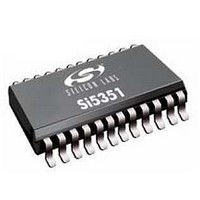
Si5351B-A-GU Silicon Laboratories Inc, Si5351B-A-GU Datasheet - Page 14

Si5351B-A-GU
Manufacturer Part Number
Si5351B-A-GU
Description
Clock Generators & Support Products AnyRate 2 PLL 125MHz Clk w/VCXO&I2C 8out
Manufacturer
Silicon Laboratories Inc
Type
Any Frequency CMOS Clock Generatorr
Specifications of Si5351B-A-GU
Mounting Style
SMD/SMT
Max Input Freq
0.008 MHz
Max Output Freq
133 MHz
Number Of Outputs
8
Operating Supply Voltage
3.3 V
Operating Temperature Range
- 40 C to + 85 C
Supply Current
25 mA
Package / Case
QSOP-24
Lead Free Status / RoHS Status
Lead free / RoHS Compliant
Si5351A/B/C
4. I
Many of the functions and features of the Si5351 are controlled by reading and writing to the RAM space using the
I
summary of register functions is shown in Section 7.
The I
Fast-Mode (400 kbps) and supports burst data transfer with auto address increments.
The I
Both the SDA and SCL pins must be connected to the VDD supply via an external pull-up as recommended by the
I
The 7-bit device (slave) address of the Si5351 consist of a 6-bit fixed address plus a user selectable LSB bit as
shown in Figure 8. The LSB bit is selectable as 0 or 1 using the optional A0 pin which is useful for applications that
require more than one Si5351 on a single I
Data is transferred MSB first in 8-bit words as specified by the I
bit device (slave) address + a write bit, an 8-bit register address, and 8 bits of data as shown in Figure 9. A write
burst operation is also shown where every additional data word is written using to an auto-incremented address.
14
2
2
C interface. The following is a list of the common features that are controllable through the I
C specification.
Read Status Indicators
Configuration of multiplication and divider values for the PLLs, MultiSynth dividers
Configuration of the Spread Spectrum profile (down or center spread, modulation percentage)
Control of the cross point switch selection for each of the PLLs and MultiSynth dividers
Set output clock options
2
2
2
Loss of signal (LOS) for the CLKIN input
Loss of lock (LOL) for PLLA and PLLB
Enable/disable for each clock output
Invert/non-invert for each clock output
Output divider values (2
Output state when disabled (stop hi, stop low, Hi-Z)
Output phase offset
C interface operates in slave mode with 7-bit addressing and can operate in Standard-Mode (100 kbps) or
C bus consists of a bidirectional serial data line (SDA) and a serial clock input (SCL) as shown in Figure 7.
C Interface
n
I
, n=1.. 7)
2
C Bus
Pull-down to GND (A0 = 0)
I
Pull-up to VDD (A0 = 1)
2
C Address Select:
Slave Address
Figure 8. Si5351 I
Figure 7. I
4.7 k
>1k
2
VDD
C bus.
Preliminary Rev. 0.95
INTR
>1k
SDA
SCL
A0
2
1
6
C and Control Signals
1
5
4
0
2
C Slave Address
0
3
2
0
2
C specification. A write command consists of a 7-
0 0/1
1
Si5351
0
A0
2
C interface. A


