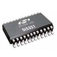
Si5351B-A-GU Silicon Laboratories Inc, Si5351B-A-GU Datasheet - Page 21

Si5351B-A-GU
Manufacturer Part Number
Si5351B-A-GU
Description
Clock Generators & Support Products AnyRate 2 PLL 125MHz Clk w/VCXO&I2C 8out
Manufacturer
Silicon Laboratories Inc
Type
Any Frequency CMOS Clock Generatorr
Specifications of Si5351B-A-GU
Mounting Style
SMD/SMT
Max Input Freq
0.008 MHz
Max Output Freq
133 MHz
Number Of Outputs
8
Operating Supply Voltage
3.3 V
Operating Temperature Range
- 40 C to + 85 C
Supply Current
25 mA
Package / Case
QSOP-24
Lead Free Status / RoHS Status
Lead free / RoHS Compliant
Si5351A/B/C
6. Design Considerations
The Si5351 is a self-contained clock generator that requires very few external components. The following general
guidelines are recommended to ensure optimum performance. Refer to “AN554: Si5350/51 PCB Layout Guide” for
additional layout recommendations.
6.1. Power Supply Decoupling/Filtering
The Si5351 has built-in power supply filtering circuitry and extensive internal Low Drop Out (LDO) voltage
regulators to help minimize the number of external bypass components. All that is recommended is one 0.1 µF
decoupling capacitor per power supply pin. This capacitor should be mounted as close to the VDD and VDDOx
pins as possible without using vias.
6.2. Power Supply Sequencing
The VDD and VDDOx (i.e., VDDO0, VDDO1, VDDO2, VDDO3) power supply pins have been separated to allow
flexibility in output signal levels. If a minimum output-to-output skew is important, then all VDDOx must be applied
before VDD. Unused VDDOx pins should be tied to VDD.
6.3. External Crystal
The external crystal should be mounted as close to the pins as possible using short PCB traces. The XA and XB
traces should be kept away from other high-speed signal traces. See “AN551: Crystal Selection Guide” for more
details.
6.4. External Crystal Load Capacitors
The Si5351 provides the option of using internal and external crystal load capacitors. If internal load capacitance is
insufficient, capacitors of value < 2 pF may be used to increased equivalent load capacitance. If external load
capacitors are used, they should be placed as close to the XA/XB pads as possible. See AN554 for more details.
6.5. Unused Pins
Unused voltage control pin should be tied to GND.
Unused CLKIN pin should be tied to GND.
Unused XA/XB pins should be left floating. Refer to "5.6. Replacing a Crystal with a Clock" on page 20 when using
XA as a clock input pin.
Unused output pins (CLK0–CLK7) should be left floating.
Unused VDDOx pins should be tied to VDD.
Preliminary Rev. 0.95
21


