CBTV4010EE NXP Semiconductors, CBTV4010EE Datasheet - Page 2
CBTV4010EE
Manufacturer Part Number
CBTV4010EE
Description
Clock Drivers & Distribution 10BIT DDR SDRAM MUX BUS SWITCH
Manufacturer
NXP Semiconductors
Datasheet
1.CBTV4010EE.pdf
(10 pages)
Specifications of CBTV4010EE
Maximum Data Rate
0.4 Gbps
Minimum Operating Temperature
0 C
Mounting Style
SMD/SMT
Multiply / Divide Factor
4:1
Number Of Clock Inputs
10
Supply Voltage (max)
2.7 V
Supply Voltage (min)
2.3 V
Maximum Operating Temperature
+ 85 C
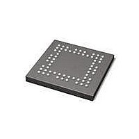
Package / Case
TFBGA-64
Lead Free Status / RoHS Status
Lead free / RoHS Compliant
Other names
CBTV4010EE,557
Available stocks
Company
Part Number
Manufacturer
Quantity
Price

Part Number:
CBTV4010EE
Manufacturer:
PHI
Quantity:
20 000
Company:
Part Number:
CBTV4010EE,551
Manufacturer:
NXP Semiconductors
Quantity:
10 000
Company:
Part Number:
CBTV4010EE,557
Manufacturer:
NXP Semiconductors
Quantity:
10 000


Philips Semiconductors
FEATURES
QUICK REFERENCE DATA
ORDERING INFORMATION
TFBGA64 (Thin Fine Pitch BGA)
2002 Feb 19
Enable signal is SSTL_2 compatible
Optimized for use in Double Data Rate (DDR) SDRAM
applications
Designed to be used with 400 Mbps/200 MHz DDR data bus
Switch on resistance is designed to eliminate the need for series
resistor to DDR SDRAM
20
Internal 100
Low differential skew
Matched rise/fall slew rate
Low cross-talk data-data/data-DQM
Independent DIMM control lines
Latch-up protection exceeds 500 mA per JESD78
ESD protection exceeds 2000 V HBM per JESD22-A114,
200 V MM per JESD22-A115 and 1000 V CDM per JESD22-C101
10-bit DDR SDRAM mux/bus switch
SYMBOL
C
I
t
t
C
on resistance
PLH
PHL
CCZ
ON
IN
PACKAGES
pull-down resistors
Propagation delay
An to Yn
Input capacitance – control pins
Channel on capacitance
Total supply current
PARAMETER
TEMPERATURE RANGE
0 to +85 C
C
V
V
V
I
in
CC
L
= 0 V or V
= 7 pF; V
= 1.5 V
= 2.5 V
2
CC
CC
T
amb
= 2.5 V
DESCRIPTION
This 10-bit bus switch is designed for 2.3 V to 2.7 V V
and SSTL_2 select input levels.
Each Host port pin is multiplexed to one of four DIMM port pins.
When the S pin is low the corresponding 10-bit bus switch is turned
on. The on-state connects the Host port to the DIMM port through a
20
open and a high-impedance state exists between the two ports. The
DIMM port is terminated with a 100
S pin is high. The design is intended to have only one DIMM port
active at any time.
The part incorporates a very low cross-talk design. It has a very low
skew between outputs (< 50 ps) and low skew (< 50 ps) for rising
and falling edges. The part has optional performance in DDR data
bus applications.
Each switch has been optimized for connection to 1 or 2-bank
DIMMs.
The low internal RC time constant of the switch (20
data transfer to be made with minimal propagation delay.
The CBTV4010 is characterized for operation from 0 to +85 C.
= 25 C; GND = 0 V
CONDITIONS
nominal series resistance. When the S pin is high the switch is
ORDER CODE
CBTV4010EE
resistor to ground when the
TYPICAL
140
500
1.8
7
CBTV4010
DWG NUMBER
SOT746-1
853-2315 27756
CC
Product data
7 pF) allows
operation
UNIT
pF
pF
ps
A
Related parts for CBTV4010EE
Image
Part Number
Description
Manufacturer
Datasheet
Request
R

Part Number:
Description:
NXP Semiconductors designed the LPC2420/2460 microcontroller around a 16-bit/32-bitARM7TDMI-S CPU core with real-time debug interfaces that include both JTAG andembedded trace
Manufacturer:
NXP Semiconductors
Datasheet:

Part Number:
Description:
NXP Semiconductors designed the LPC2458 microcontroller around a 16-bit/32-bitARM7TDMI-S CPU core with real-time debug interfaces that include both JTAG andembedded trace
Manufacturer:
NXP Semiconductors
Datasheet:
Part Number:
Description:
NXP Semiconductors designed the LPC2468 microcontroller around a 16-bit/32-bitARM7TDMI-S CPU core with real-time debug interfaces that include both JTAG andembedded trace
Manufacturer:
NXP Semiconductors
Datasheet:
Part Number:
Description:
NXP Semiconductors designed the LPC2470 microcontroller, powered by theARM7TDMI-S core, to be a highly integrated microcontroller for a wide range ofapplications that require advanced communications and high quality graphic displays
Manufacturer:
NXP Semiconductors
Datasheet:
Part Number:
Description:
NXP Semiconductors designed the LPC2478 microcontroller, powered by theARM7TDMI-S core, to be a highly integrated microcontroller for a wide range ofapplications that require advanced communications and high quality graphic displays
Manufacturer:
NXP Semiconductors
Datasheet:
Part Number:
Description:
The Philips Semiconductors XA (eXtended Architecture) family of 16-bit single-chip microcontrollers is powerful enough to easily handle the requirements of high performance embedded applications, yet inexpensive enough to compete in the market for hi
Manufacturer:
NXP Semiconductors
Datasheet:
Part Number:
Description:
The XA-S3 device is a member of Philips Semiconductors? XA(eXtended Architecture) family of high performance 16-bitsingle-chip microcontrollers
Manufacturer:
NXP Semiconductors
Datasheet:

Part Number:
Description:
The NXP BlueStreak LH75401/LH75411 family consists of two low-cost 16/32-bit System-on-Chip (SoC) devices
Manufacturer:
NXP Semiconductors
Datasheet:
Part Number:
Description:
The NXP LPC3130/3131 combine an 180 MHz ARM926EJ-S CPU core, high-speed USB2
Manufacturer:
NXP Semiconductors
Datasheet:
Part Number:
Description:
The NXP LPC3141 combine a 270 MHz ARM926EJ-S CPU core, High-speed USB 2
Manufacturer:
NXP Semiconductors
Part Number:
Description:
The NXP LPC3143 combine a 270 MHz ARM926EJ-S CPU core, High-speed USB 2
Manufacturer:
NXP Semiconductors

Part Number:
Description:
The NXP LPC3152 combines an 180 MHz ARM926EJ-S CPU core, High-speed USB 2
Manufacturer:
NXP Semiconductors
Part Number:
Description:
The NXP LPC3154 combines an 180 MHz ARM926EJ-S CPU core, High-speed USB 2
Manufacturer:
NXP Semiconductors

Part Number:
Description:
Standard level N-channel enhancement mode Field-Effect Transistor (FET) in a plastic package using NXP High-Performance Automotive (HPA) TrenchMOS technology
Manufacturer:
NXP Semiconductors
Datasheet: