LAN91C96I-MU SMSC, LAN91C96I-MU Datasheet
LAN91C96I-MU
Specifications of LAN91C96I-MU
Available stocks


Related parts for LAN91C96I-MU


LAN91C96I-MU Summary of contents
Page 1
... Fast Access Time Pipelined Data Path Handles Block Word Transfers for any Alignment 1 Refer to Description of Pin Functions on Page 17 for 5V tolerant pins SMSC LAN91C96 5v&3v LAN91C96 Non-PCI Single-Chip Full Duplex Ethernet Controller with Magic Packet High Performance Chained ("Back-to-Back") Transmit and Receive ...
Page 2
... Any and all such uses without prior written approval of an Officer of SMSC and further testing and/or modification will be fully at the risk of the customer. Copies of this document or other SMSC literature, as well as the Terms of Sale Agreement, may be obtained by visiting SMSC’s website at http://www.smsc.com. SMSC is a registered trademark of Standard Microsystems Corporation (“ ...
Page 3
... I/O Space Registers Description ....................................................................................................................42 CHAPTER 8 THEORY OF OPERATION ................................................................... 65 8.1 Typical Flow of Events for Transmit (Auto Release = 0) ............................................................................67 8.2 Typical Flow of Events for Transmit (Auto Release = 1) ............................................................................68 8.3 Flow of Events for Receive .............................................................................................................................69 CHAPTER 9 FUNCTIONAL DESCRIPTION OF THE BLOCKS................................ 79 SMSC LAN91C96 5v&3v Page 3 DATASHEET Revision 1.0 (10-24-08) ...
Page 4
... CHAPTER 10 BOARD SETUP INFORMATION ........................................................ 89 10.1 Diagnostic LEDs ..........................................................................................................................................90 10.2 Bus Clock Considerations...........................................................................................................................90 10.3 68000 Bus Interface.....................................................................................................................................90 CHAPTER 11 OPERATIONAL DESCRIPTION ......................................................... 92 11.1 Maximum Guaranteed Ratings* ................................................................................................................92 11.2 DC Electrical Characteristics.....................................................................................................................92 Revision 1.0 (10-24-08) Non-PCI Single-Chip Full Duplex Ethernet Controller with Magic Packet Page 4 DATASHEET Datasheet SMSC LAN91C96 5v&3v ...
Page 5
... Figure 12.25 – Memory Read Timing.........................................................................................................................121 Figure 12.26 – Input Clock Timing .............................................................................................................................122 Figure 12.27 – Memory Write Timing .........................................................................................................................122 Figure 12.28 - 100 PIN QFP Package........................................................................................................................123 Figure 12.29 - 100 PIN TQFP Package .....................................................................................................................124 SMSC LAN91C96 5v&3v Page 5 DATASHEET Revision 1.0 (10-24-08) ...
Page 6
... Table 5.7- LOCAL BUS Mode ......................................................................................................................................33 Table 5.8 - PCMCIA Mode (Refer To Table 5.7 For Next States To Wake-Up Events) ...............................................34 Table 5.9 - PCMCIA Mode ...........................................................................................................................................34 Table 7.1 - Transmit Loop ............................................................................................................................................45 Revision 1.0 (10-24-08) Non-PCI Single-Chip Full Duplex Ethernet Controller with Magic Packet Page 6 DATASHEET Datasheet SMSC LAN91C96 5v&3v ...
Page 7
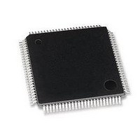
... The LAN91C96 is available in 100-pin QFP and TQFP (1.0 mm body thickness) packages. The low profile TQFP is ideal for mobile applications such as PC Card LAN adapters. The LAN91C96 operates with a single power supply voltage of 5.0V. Revisions E and later will also operate using a single 3.3V power supply. SMSC LAN91C96 5v&3v Page 7 DATASHEET Revision 1.0 (10-24-08) ...
Page 8
... ROM is required for CIS storage. THE LAN91C96 OFFERS: High integration: Single chip controller including: Packet RAM LOCAL BUS interface Revision 1.0 (10-24-08) Non-PCI Single-Chip Full Duplex Ethernet Controller with Magic Packet The LAN91C96 integrates most of the 802.3 Page 8 DATASHEET Datasheet SMSC LAN91C96 5v&3v ...
Page 9
... PCMCIA I/O ignores address lines A4-A15 and relies on the PCMCIA host, decoding for the slot. nROM/nPCMCIA, on LAN91C96, is left open with a pullup for LOCAL BUS mode. This pin is sampled at the end of RESET. If found low, the LAN91C96 is configured for PCMCIA mode. SMSC LAN91C96 5v&3v Page 9 DATASHEET Revision 1.0 (10-24-08) ...
Page 10
... Note: The first write to the 68000 configured controller must be a write. Revision 1.0 (10-24-08) Non-PCI Single-Chip Full Duplex Ethernet Controller with Magic Packet Page 10 DATASHEET Datasheet SMSC LAN91C96 5v&3v ...
Page 11
... AVSS 89 RBIAS 90 AVDD 91 nXENDEC 92 nEN16 93 VSS 94 nROM/nPCMCIA 95 XTAL1 96 XTAL2 97 IOS0 98 IOS1 99 VDD 100 2122 2728 29 30 SMSC LAN91C96 5v&3v LAN91C96 100 Pin QFP Figure 3.1 - LAN91C96 100 Pin QFP Page 11 DATASHEET 50 VDD 49 A19/nCE1 48 A18 47 A17 46 A16 45 A15 44 A14 43 A13 42 A12 41 A11/nFCS ...
Page 12
... Non-PCI Single-Chip Full Duplex Ethernet Controller with Magic Packet LAN91C96 100 Pin TQFP Figure 3.2 - LAN91C96 100 Pin TQFP Page 12 DATASHEET Datasheet 75 TPETXP 74 TPETXDN 73 TPETXN 72 TPETXDP 71 AVDD 70 nTXLED/nTXEN 69 nRXLED/RXCLK 68 nLNKLED/TXD 67 nBSELED/RXD 66 PWRDWN/TXCLK 65 RESET 64 VSS VDD VSS 53 IOCHRDY/nWAIT 52 AEN/nREG/nAS 51 nMEMR/OE SMSC LAN91C96 5v&3v ...
Page 13
... Non-PCI Single-Chip Full Duplex Ethernet Controller with Magic Packet Datasheet PCMCIA CONNECTOR nWE nOE D0-7 A0-X SINGLE FUNCTION PCMCIA CARD WITH THE LAN91C96 Figure 3.3 - LAN91C96 System Block Diagram SMSC LAN91C96 5v&3v nCE1, nCE2, nREG, nWE A0-9, A15 nIORD, nIOWR STSCHG RESET LAN91C96 nIREQ D0-15 nIOIS16, nINPACK ...
Page 14
... CABLE SIDE DIAGNOSTIC LEDs Figure 3.4 – System Diagram for Local Bus with Boot Prom Revision 1.0 (10-24-08) Non-PCI Single-Chip Full Duplex Ethernet Controller with Magic Packet AUI Page 14 DATASHEET Datasheet SMSC LAN91C96 5v&3v ...
Page 15
... GND, AGND 10BASE-T interface TPERXP TPERXN TPETXP TPETXN TPETXDP TPETXDN AUI interface RECP RECN COLP COLN TXP/nCOLL TXN/nCRS 2 The bytes connect to the 68000 host processor swapped SMSC LAN91C96 5v&3v PCMCIA A0 A1-9 A1-9 nFWE A10 nFCS A11 A12-14 A15 A15 A16-18 nCE1 A19 ...
Page 16
... Revision 1.0 (10-24-08) Non-PCI Single-Chip Full Duplex Ethernet Controller with Magic Packet PCMCIA nLNKLED/TXD nLNKLED/TXD nRXLED/RXCLK nRXLED/RXCLK nBSELED/RXD nBSELED/RXD nTXLED/nTXEN nTXLED/nTXEN RBIAS RBIAS PWRDWN/TX PWRDWN/TXC CLK LK nXENDEC nXENDEC nEN16 nEN16 nROM nPCMCIA Page 16 DATASHEET Datasheet MAX 68000 NUMBER OF PINS 4 5 SMSC LAN91C96 5v&3v ...
Page 17
... IOCHRDY/ nWAIT SMSC LAN91C96 5v&3v TYPE DESCRIPTION I/O4 with This pin is sampled at the end of RESET. When this pullup pin is sampled low the LAN91C96 is configured for PCMCIA operation and all pin definitions correspond to the PCMCIA mode. For LOCAL BUS operation this ...
Page 18
... LAN91C96 bit mode, COR0 bit is high and nREG is low. IS with LOCAL BUS, PCMCIA - Input. Active low read strobe pullup used to access the LAN91C96 IO space. ** 68000 – Data strobe input. UDS, LDS can be tied to this pin. Page 18 DATASHEET Datasheet SMSC LAN91C96 5v&3v ...
Page 19
... RXCLK 68 70 nLNKLED/ TXD 1 3 ENEEP SMSC LAN91C96 5v&3v TYPE DESCRIPTION IS with LOCAL BUS, PCMCIA - Input. Active low write strobe pullup used to access the LAN91C96 IO space. ** 68000 – Read/nWrite strobe to read from or write to the chip. IS with LOCAL BUS - Active low signal used by the host pullup processor to read from the external ROM ...
Page 20
... EXTERNAL ENDEC. When tied high or left open the LAN91C96 will use its internal encoder/decoder. ** +5V power supply pins or 3.3V power supply pins (Revisions E and later) +5V analog power supply pins or 3.3V power supply pins (Revisions E and later) Page 20 DATASHEET Datasheet SMSC LAN91C96 5v&3v ...
Page 21
... Input buffer with TTL levels. IS Input buffer with Schmitt Trigger Hysteresis. Iclk Clock input buffer. ** Signal is 5.0V input tolerant when V DC levels and conditions defined in the DC Electrical Characteristics section. SMSC LAN91C96 5v&3v TYPE DESCRIPTION Ground pins. Analog ground pins. =3.3V. For Revision E and later. cc Page 21 DATASHEET Revision 1 ...
Page 22
... DATABU ADDRES BUS BUS INTERFAC CONTROL Figure 4.1 - LAN91C96 Internal Block Diagram Revision 1.0 (10-24-08) Non-PCI Single-Chip Full Duplex Ethernet Controller with Magic Packet ARBITE CSMA/C MMU TWISTED TRANSCEIVE RAM Page 22 DATASHEET Datasheet ENDE AUI 10BASE- SMSC LAN91C96 5v&3v ...
Page 23
... MMU. Byte and word accesses to the RAM are supported. If the system to SRAM bandwidth is insufficient the LAN91C96 will automatically use its IOCHRDY line for flow control. However, for LOCAL BUS, IOCHRDY will never be negated. SMSC LAN91C96 5v&3v Page 23 DATASHEET Revision 1.0 (10-24-08) ...
Page 24
... The FIFO of packets, existing beneath the TX and RX areas, is managed by the MMU. The MMU dynamically allocates and releases memory to be used by the transmit and receive functions. Revision 1.0 (10-24-08) Non-PCI Single-Chip Full Duplex Ethernet Controller with Magic Packet 6kbytes 24 24 (FIFOs have 24 entries of 5 bits) 6 256 bytes Page 24 DATASHEET Datasheet SMSC LAN91C96 5v&3v ...
Page 25
... Non-PCI Single-Chip Full Duplex Ethernet Controller with Magic Packet Datasheet Figure 5.1 – Mapping and Paging vs. Receive and Transmit Area SMSC LAN91C96 5v&3v Page 25 DATASHEET Revision 1.0 (10-24-08) ...
Page 26
... Figure 5.2 – Transmit Queues and Mapping Revision 1.0 (10-24-08) Non-PCI Single-Chip Full Duplex Ethernet Controller with Magic Packet Page 26 DATASHEET Datasheet SMSC LAN91C96 5v&3v ...
Page 27
... Non-PCI Single-Chip Full Duplex Ethernet Controller with Magic Packet Datasheet Figure 5.3 – Receive Queues and Mapping SMSC LAN91C96 5v&3v Page 27 DATASHEET Revision 1.0 (10-24-08) ...
Page 28
... Non-PCI Single-Chip Full Duplex Ethernet Controller with Magic Packet Control Control Control Arbiter Ethernet Protocol Handler MMU TX/RX DMA FIFO Pointer TX Data TX Data 6K Byte SRAM RX Data RX Data Page 28 DATASHEET Datasheet ENDEC AUI (EPH) TPO Twisted Pair Transceiver TPI SMSC LAN91C96 5v&3v ...
Page 29
... Non-PCI Single-Chip Full Duplex Ethernet Controller with Magic Packet Datasheet Figure 5.5 – Logical Address Generation and Relevant Registers SMSC LAN91C96 5v&3v Page 29 DATASHEET Revision 1.0 (10-24-08) ...
Page 30
... Page 30 DATASHEET Datasheet ON- DEPTH WIDTH CHIP 32k 8 bits on locations, even (extern only even addresses al bytes are ROM) usable bits locations, only even bytes are usable Y 16 locations bits (68K: 16 bits only) D8- Odd byte - - Odd byte Invalid cycle SMSC LAN91C96 5v&3v ...
Page 31
... Ethernet core. The enabling, reporting, and clearing of these sources is controlled by the ECOR register. The interrupt structure is similar for LOCAL BUS and PCMCIA modes with the following exceptions: PCMCIA uses a single interrupt pin (nIREQ) while LOCAL BUS can use any of four INTR0-3 pins. SMSC LAN91C96 5v&3v NCE1 NCE2 D0-7 ...
Page 32
... OR function of all interrupt bits specified in the Interrupt Status Register ANDed with their respective Enable bits Intr bit in ECSR LOCAL BUS FUNCTIONS VS. PCMCIA Page 32 DATASHEET Datasheet LOCAL BUS MODE INTR0-3 Not Applicable in LOCAL BUS mode SAMPLES TRIGGERS EEPROM READ MODE Yes Yes No Yes No No SMSC LAN91C96 5v&3v The ...
Page 33
... By writing CTR WAKEUP_EN bit AND CTR PWRDWN bit = 0 ..5 By writing 0 to CTR PWRDWN bit Notes: The chart assumes that ECOR Function Enable bit is meaningless in LOCAL BUS mode. SMSC LAN91C96 5v&3v CURRENT STATE CTR ECSR CTR WAKEU POWER PWRDW P_EN DOWN ...
Page 34
... Mem Ethernet Tx, PCMCIA Att/Config Rx, Link Mem Ethernet Tx, PCMCIA Att/Config Link Mem Ethernet Tx, PCMCIA Att/Config Link Mem CTR CTR PWRDWN WAKEUP_EN COMMENTS BIT BIT No change No change Pin deassertion will make the Att/Conf Mem accessible entirely 0 0 Fully Awake 0 0 SMSC LAN91C96 5v&3v ...
Page 35
... PCMCIA requiring a Minimum size bit word addresses. The LAN91C96 generates the appropriate control lines (nFCS and nFWE) to read and write the Attribute memory, and it tri-states the data bus during external Attribute Memory accesses. Only even locations are used. SMSC LAN91C96 5v&3v NEXT STATE ECOR ECSR ...
Page 36
... Ethernet I/O space (i.e. The bank Revision 1.0 (10-24-08) Non-PCI Single-Chip Full Duplex Ethernet Controller with Magic Packet EXTERNAL EPROM CONFIGURATIO STORE ATTRIB Page 36 DATASHEET Datasheet N REGISTERS Enable Function 0 0 SMSC LAN91C96 5v&3v ...
Page 37
... Ethernet function is also put into power down mode when the Enable Function bit (ECOR bit 0 in PCMCIA only) is cleared. Refer to the Power Down Logic section for additional information. BIT 1 - Intr: This bit is read/set to a one when this function is requesting interrupt service. When this bit is set, IREQOut is asserted. BIT 0 - Not Defined SMSC LAN91C96 5v& ...
Page 38
... Status Register) Written by CPU Written/modified by CPU Written by CPU to control ODD/EVEN data bytes Page 38 DATASHEET Datasheet bit0 1st Byte RECEIVE PACKET Written by CSMA upon receive completion (see RX Frame Status Word) Written by CSMA Written by CSMA Written by CSMA. Also has ODD/EVEN bit SMSC LAN91C96 5v&3v ...
Page 39
... This word is written at the beginning of each receive frame in memory not available as a register. ALGN BROD ERR CAST 5 ALGNERR - Frame had alignment error. BRODCAST - Receive frame was broadcast. BADCRC - Frame had CRC error. SMSC LAN91C96 5v&3v ODD CRC 0 ODD 0 0 BADCRC ODDFRM ...
Page 40
... Revision 1.0 (10-24-08) Non-PCI Single-Chip Full Duplex Ethernet Controller with Magic Packet HASH VALUE 5-0 MULTICAST TABLE BIT 000 000 MT-0 bit 0 010 000 MT-2 bit 0 100 111 MT-4 bit 7 111 111 MT-7 bit 7 Page 40 DATASHEET Datasheet SMSC LAN91C96 5v&3v ...
Page 41
... Non-PCI Single-Chip Full Duplex Ethernet Controller with Magic Packet Datasheet SMSC LAN91C96 5v&3v Figure 6.2 - LAN91C96 Registers Page 41 DATASHEET Revision 1.0 (10-24-08) ...
Page 42
... BIT 10 RST RST RST RST Val Val Val Val BIT 5 BIT 4 BIT 3 BIT 2 RST RST RST RST Val Val Val Val Page 42 DATASHEET Datasheet SYMBOL BSR BIT9 BIT8 RST RST Val Val BIT 1 BIT 0 RST RST Val Val SMSC LAN91C96 5v&3v ...
Page 43
... LOCAL BUS and PCMCIA mode. BS2 I/O SPACE - BANK0 OFFSET 0 TRANSMIT CONTROL REGISTER This register holds bits programmed by the CPU to control some of the protocol transmit options. FDSE Reserved 0 0 PAD_EN 0 X SMSC LAN91C96 5v&3v NAME TYPE BANK SELECT READ/WRITE REGISTER ...
Page 44
... TXENA - Transmit enabled when set. Transmit is disabled if clear. When the bit is cleared the LAN91C96 will complete the current transmission before stopping. When stopping due to an error, this bit is automatically cleared. Revision 1.0 (10-24-08) Non-PCI Single-Chip Full Duplex Ethernet Controller with Magic Packet Page 44 DATASHEET Datasheet SMSC LAN91C96 5v&3v ...
Page 45
... LATCOL - Late collision detected on last transmit frame. If set a late collision was detected (later than 64 byte times into the frame). When detected the transmitter JAMs and turns itself off clearing the TXENA bit in TCR. Cleared by setting TXENA in TCR. SMSC LAN91C96 5v&3v Table 7.1 - Transmit Loop EPH_LOOP ...
Page 46
... Registers. The EEPROM in both LOCAL BUS and PCMCIA mode is not reloaded after software reset. Revision 1.0 (10-24-08) Non-PCI Single-Chip Full Duplex Ethernet Controller with Magic Packet NAME READ/WRITE ALMUL Page 46 DATASHEET Datasheet TYPE SYMBOL RCR 0 STRIP RXEN CRC PRMS RX_ ABORT SMSC LAN91C96 5v&3v ...
Page 47
... The COUNTER REGISTER facilitates maintaining statistics in the AUTO RELEASE mode where no transmit interrupts are generated on successful transmissions. Reading the register in the transmit service routine will be enough to maintain statistics. SMSC LAN91C96 5v&3v NAME COUNTER REGISTER NUMBER OF DEFERRED TX ...
Page 48
... UPPER BYTE READ ONLY Memory Size Multiplier “M” When programmed for a non-zero value, the Page 48 DATASHEET Datasheet TYPE SYMBOL READ ONLY MIR ACTUAL MEMORY 1 64 kbytes 1 16 kbytes 1 4608 bytes 1 6144 bytes 1 6144 bytes 2 128 kbytes TYPE SYMBOL MCR SMSC LAN91C96 5v&3v ...
Page 49
... LINK_OK bit will be set and the LINK LED will stay on. When low the link test functions are enabled. If the link status indicates FAIL, the EPHSR LINK_OK bit will be low, while transmit packets enqueued will be processed by the LAN91C96, transmit data will not be sent out to the cable. SMSC LAN91C96 5v&3v BIT 11 BIT 10 BIT 9 ...
Page 50
... A14 A13 A12 A11 Revision 1.0 (10-24-08) Non-PCI Single-Chip Full Duplex Ethernet Controller with Magic Packet INTERRUPT PIN USED INTR0 INTR1 INTR2 INTR3 NAME READ/WRITE A13 RA18 RA17 RA16 A10 Page 50 DATASHEET Datasheet TYPE SYMBOL BAR RA15 RA14 SMSC LAN91C96 5v&3v ...
Page 51
... EEPROM reload. The registers can be modified by the software driver, but a STORE operation will not modify the EEPROM Individual Address contents. Bit 0 of Individual Address 0 register corresponds to the first bit of the address on the cable SMSC LAN91C96 5v&3v NAME READ/WRITE ADDRESS ADDRESS ADDRESS 2 0 ...
Page 52
... Non-PCI Single-Chip Full Duplex Ethernet Controller with Magic Packet NAME HIGH DATA BYTE LOW DATA BYTE NAME CONTROL REGISTER WAKEUP AUTO _EN RELEAS Page 52 DATASHEET Datasheet TYPE SYMBOL READ/WRITE GPR TYPE SYMBOL READ/WRITE CTR EEPROM RELOAD STORE SELECT SMSC LAN91C96 5v&3v ...
Page 53
... EEPROM status, will NOT have any effect on the internal registers. The CPU can resume accesses to the LAN91C96 after both bits are low. A worst case RELOAD operation initiated by RESET or by software takes less than 750usec in either mode. SMSC LAN91C96 5v&3v Page 53 DATASHEET ...
Page 54
... Typically used to remove transmitted frames, after reading their completion status. Revision 1.0 (10-24-08) Non-PCI Single-Chip Full Duplex Ethernet Controller with Magic Packet NAME WRITE ONLY BUSY bit readable Reserved Reserved Reserved Page 54 DATASHEET Datasheet TYPE SYMBOL MMUCR Reserved Reserved N0 BUSY 0 will request SMSC LAN91C96 5v&3v 2 ...
Page 55
... PACKET NUMBER AT TX AREA - The value written into this register determines which packet number is accessible through the TX area. Some MMU commands use the number stored in this register as the packet number parameter. This register is cleared by a RESET or a RESET MMU Command. RESERVED – This bit is reserved. SMSC LAN91C96 5v&3v NAME TYPE READ/WRITE ...
Page 56
... PNR as is, without masking higher bits (provided TEMPTY and REMPTY = 0 respectively). Revision 1.0 (10-24-08) Non-PCI Single-Chip Full Duplex Ethernet Controller with Magic Packet NAME READ ONLY ALLOCATED PACKET NUMBER NAME READ ONLY RX FIFO PACKET NUMBER FIFO PACKET NUMBER Page 56 DATASHEET Datasheet TYPE SYMBOL ARR TYPE SYMBOL FIFO SMSC LAN91C96 5v&3v ...
Page 57
... Reserved – Must AUTO INCR. is not set, the pointer must be loaded with an even value. I/O SPACE - BANK2 OFFSET 8 & A DATA REGISTER - Used to read or write the data buffer byte/word presently addressed by the pointer register. SMSC LAN91C96 5v&3v NAME POINTER REGISTER Reserved Reserved 0 0 ...
Page 58
... INT INT MASK MASK MASK Page 58 DATASHEET Datasheet TYPE SYMBOL READ ONLY IST TX EMPTY INT TX INT RCV INT TYPE SYMBOL WRITE ONLY ACK TX EMPTY INT TX INT TYPE SYMBOL READ/WRITE MSK TX EMPTY INT TX INT RCV INT MASK MASK MASK SMSC LAN91C96 5v&3v ...
Page 59
... ALLOC INT - Set when an MMU request for TX ram pages is successful. This bit is the complement of the FAILED bit in the ALLOCATION RESULT register. The ALLOC INT bit is cleared by the MMU when the next allocation request is processed or allocation fails. SMSC LAN91C96 5v&3v Page 59 DATASHEET ...
Page 60
... For edge triggered systems, the Interrupt Service Routine should clear the Interrupt Mask Register, and only enable the appropriate interrupts after the interrupt source is serviced (acknowledged). Revision 1.0 (10-24-08) Non-PCI Single-Chip Full Duplex Ethernet Controller with Magic Packet Page 60 DATASHEET Datasheet SMSC LAN91C96 5v&3v ...
Page 61
... Non-PCI Single-Chip Full Duplex Ethernet Controller with Magic Packet Datasheet SMSC LAN91C96 5v&3v Figure 7.1 – Interrupt Structure Page 61 DATASHEET Revision 1.0 (10-24-08) ...
Page 62
... MULTICAST TABLE READ/WRITE Multicast Table Multicast Table Multicast Table Multicast Table Multicast Table Multicast Table Multicast Table Multicast Table NAME READ/WRITE nXNDEC IOS2 1 1 MDOE MCLK Page 62 DATASHEET Datasheet TYPE SYMBOL TYPE SYMBOL MGMT IOS1 IOS0 MDI MD0 SMSC LAN91C96 5v&3v ...
Page 63
... REV - Revision ID. Incremented for each revision of a given device. Note 7.2 The LAN91C96 shares the same chip ID (#4) as the LAN91C94. The Rev. ID for the LAN91C96 will begin from six (#6). SMSC LAN91C96 5v&3v MODE=0 Serial EEPROM Data Out Serial EEPROM Clock Serial EEPROM Chip Select ...
Page 64
... Counter register will return a value of “0” when no receive event is occurring. Revision 1.0 (10-24-08) Non-PCI Single-Chip Full Duplex Ethernet Controller with Magic Packet NAME RCV REGISTER READ/WRITE RCV COUNTER MBO MBO MBO Page 64 DATASHEET Datasheet TYPE SYMBOL RCV 1 1 MBO MBO 1 1 SMSC LAN91C96 5v&3v ...
Page 65
... Behavior in FDSE mode A) No deferral - The transmit channel is dedicated and always available - The device transmits whenever it has a packet ready to be sent, while respecting the interframe spacing between transmit packets. SMSC LAN91C96 5v&3v Page 65 DATASHEET The loopback (Full Duplex for ...
Page 66
... The Interrupt bit in the ECSR is also set if the host plans on polling the controller for Wakeup status. Revision 1.0 (10-24-08) Non-PCI Single-Chip Full Duplex Ethernet Controller with Magic Packet Page 66 DATASHEET Datasheet SMSC LAN91C96 5v&3v ...
Page 67
... Packet Number Register into the TX FIFO. The transmission is now enqueued. No further CPU intervention is needed until a transmit interrupt is generated SMSC LAN91C96 5v&3v MAC SIDE The enqueued packet will be transferred to the MAC block as a function of TXENA (nTCR) bit and of the deferral process (1/2 duplex mode only) state. ...
Page 68
... Non-PCI Single-Chip Full Duplex Ethernet Controller with Magic Packet MAC SIDE The enqueued packet will be transferred to the MAC block as a function of TXENA (nTCR) bit and of the deferral process (1/2 duplex mode only) state. Transmit pages are released by transmit completion. Page 68 DATASHEET Datasheet SMSC LAN91C96 5v&3v ...
Page 69
... When processing is complete the CPU issues the REMOVE AND RELEASE FROM TOP OF RX command to have the MMU free up the used memory and packet number. SMSC LAN91C96 5v&3v a) The MAC generates a TXEMPTY interrupt upon a completion of a sequence of enqueued packets. ...
Page 70
... Page 70 DATASHEET Datasheet Yes RX INTR? Call RXINTR Yes Write Allocated Pkt# into Packet Number Reg. Write Ad Ptr Reg. & CopyData & Source Address Enqueue Packet Set "Ready for Packet" Flag Return Buffers to Upper Layer Disable Allocation Interrupt Mask SMSC LAN91C96 5v&3v ...
Page 71
... Non-PCI Single-Chip Full Duplex Ethernet Controller with Magic Packet Datasheet SMSC LAN91C96 5v&3v RX INTR Write Ad. Ptr. Reg. & Read Word 0 from RAM Destination Yes No Multicast? Read Words from RAM for Address Filtering No Yes Address Filtering Pass? No Yes Status Word OK? Do Receive Lookahead ...
Page 72
... Write (0x00A0, (Bank2, Offset 0)); //Option 2: Re-Enqueue the packet Write (0x00C0, (Bank2, Offset 0)); Step 4.2.4: Re-Enable Transmission Temp = Read(Bank0, Offset 0); Temp = Temp2 OR 0x0001 Write (Temp2, (Bank 0, Offset 0)); Step 4.2.5: Return from the routine Figure 8.3 -TX INTR Page 72 DATASHEET Datasheet SMSC LAN91C96 5v&3v ...
Page 73
... Non-PCI Single-Chip Full Duplex Ethernet Controller with Magic Packet Datasheet TXEMPTY = 0 & TXINT = 0 (Waiting for Completion) SMSC LAN91C96 5v&3v TXEMPTY INTR Write Acknowledge Reg. with TXEMPTY Bit Set Read TXEMPTY & TX INTR TXEMPTY = X & TXINT = 1 (Everything went through (Transmission Failed) Read Pkt. # Register & Save ...
Page 74
... Write Source Address into Proper Location Copy Remaining TX Data Packet into RAM Enqueue Packet Set "Ready for Packet" Flag Return Buffers to Upper Layer Return Page 74 DATASHEET Datasheet No Store Data Buffer Pointer Clear "Ready for Packet" Flag Enable Allocation Interrupt SMSC LAN91C96 5v&3v ...
Page 75
... TX INT bit - Set whenever the TX completion FIFO is not empty. TX EMPTY INT bit - Set whenever the TX FIFO is empty. AUTO RELEASE - When set, successful transmit packets are not written into completion FIFO, and their memory is released automatically. SMSC LAN91C96 5v&3v Page 75 DATASHEET Revision 1.0 (10-24-08) ...
Page 76
... SRESET is high to allow the oscillator to run during RESET. Except for this gating function, all other uses of the RESET pin use a de-glitched version of the signal as defined in the pin description section. Revision 1.0 (10-24-08) Non-PCI Single-Chip Full Duplex Ethernet Controller with Magic Packet Page 76 DATASHEET Datasheet SMSC LAN91C96 5v&3v ...
Page 77
... Non-PCI Single-Chip Full Duplex Ethernet Controller with Magic Packet Datasheet NXENDEC PIN PWRDN PIN SMSC LAN91C96 5v&3v PWRDN BIT 0 Normal external ENDEC operation 0 Normal internal ENDEC operation 0 Powerdown - Normal mode restored by PWRDWN pin going low Powerdown - Bit is cleared by a write 1 access to any LAN91C96 register or by ...
Page 78
... Figure 8.6 – Interrupt Generation for Transmit; Receive, MMU Revision 1.0 (10-24-08) Non-PCI Single-Chip Full Duplex Ethernet Controller with Magic Packet Page 78 DATASHEET Datasheet SMSC LAN91C96 5v&3v ...
Page 79
... By the same token, CSMA/CD cycles might be postponed. The worst case CSMA/CD latency for arbiter service is one memory cycle. The arbiter uses the pointer register as the CPU provided address, and the internal DMA address from the CSMA/CD side as the addresses to be provided to the MMU. SMSC LAN91C96 5v&3v Page 79 DATASHEET ...
Page 80
... The read access time is 40ns and the cycle time is 185ns. If any one of them does not satisfy the application requirements, wait states should be added. Revision 1.0 (10-24-08) Non-PCI Single-Chip Full Duplex Ethernet Controller with Magic Packet Page 80 DATASHEET Datasheet SMSC LAN91C96 5v&3v ...
Page 81
... When a CSMA/CD cycle begins, the arbiter will route the CSMA/CD DMA addresses to the MMU as well as the packet number associated with the operation in progress. In full-duplex mode, receive and transmit requests are alternated in such a way that the CPU arbitration cycle time is not affected. SMSC LAN91C96 5v&3v Page 81 DATASHEET ...
Page 82
... CPU via the Packet Number Register. The number was previously obtained by requesting memory allocation from the MMU. The FIFO is read by the Revision 1.0 (10-24-08) Non-PCI Single-Chip Full Duplex Ethernet Controller with Magic Packet Page 82 DATASHEET Datasheet SMSC LAN91C96 5v&3v ...
Page 83
... Note that the CPU can enqueue a transmit command with a packet number that does not follow the sequence in which the MMU assigned packet numbers. For example, when a transmission failed and it is retried in software, or when a receive packet is modified and sent back to the network. SMSC LAN91C96 5v&3v Page 83 DATASHEET ...
Page 84
... In that case TXENA will be cleared and the CPU should restart the transmission by setting it again transmission is successful, TXENA stays set and the CSMA/CD is provided by the DMA block with the next packet to be transmitted. Revision 1.0 (10-24-08) Non-PCI Single-Chip Full Duplex Ethernet Controller with Magic Packet Page 84 DATASHEET Datasheet SMSC LAN91C96 5v&3v ...
Page 85
... The interface 'unjabs' when the transmitter has been idle for a minimum of 256 ms phase-lock loop to recover data and clock from the Manchester data stream with up to plus or minus 18ns of jitter. 4. Diagnostic loopback capability. 5. LED drivers for collision, transmission, reception, and jabber. SMSC LAN91C96 5v&3v Page 85 DATASHEET Revision 1.0 (10-24-08) ...
Page 86
... TPETXDP(N). Each output of the transmit driver pair has a source resistance of 10 ohms maximum and a current rating maximum. The degree of predistortion is determined by the termination resistors; the equivalent resistance should be 100 ohms. Revision 1.0 (10-24-08) Non-PCI Single-Chip Full Duplex Ethernet Controller with Magic Packet Page 86 DATASHEET Datasheet SMSC LAN91C96 5v&3v ...
Page 87
... Reverse Polarity Function In the 10BASE-T mode, the PHY monitors for receiver polarity reversal due to crossed wires and corrects by reversing the signal internally. SMSC LAN91C96 5v&3v Page 87 DATASHEET Revision 1.0 (10-24-08) ...
Page 88
... The Link Integrity function can be disabled for pre-10BASE-T twisted-pair networks. Revision 1.0 (10-24-08) Non-PCI Single-Chip Full Duplex Ethernet Controller with Magic Packet Page 88 DATASHEET Datasheet SMSC LAN91C96 5v&3v ...
Page 89
... STORE) are used to control the EEPROM. Their values are not stored nor loaded from the EEPROM. b) GENERAL PURPOSE REGISTER - EEPROM SELECT bit = 1 On EEPROM read operations (after setting RELOAD high) the EEPROM word address defined by the POINTER REGISTER 6 least significant bits is read into the GENERAL PURPOSE REGISTER. SMSC LAN91C96 5v&3v EEPROM WORD REGISTER ADDRESS IOS Value * 4 ...
Page 90
... LOCAL BUS or PCMCIA modes. The following is the Motorola 68000 Processor and the LAN91C96 pin mapping: DS, LDS, or UDS to nIORD/xDS R/nW to nIOWR/R/nW Revision 1.0 (10-24-08) Non-PCI Single-Chip Full Duplex Ethernet Controller with Magic Packet Page 90 DATASHEET Datasheet This SMSC LAN91C96 5v&3v ...
Page 91
... All INTx must have a 1KΩ to 10KΩ pull-up to keep the line high while the drivers are tri-stated. IOS2-0 000 001 010 011 100 101 110 XXX FIGURE 10 SERIAL EEPROM MAP SMSC LAN91C96 5v&3v 16 BITS DRESS 0h CONFIGURATION REG. 1h BASE REG. 4h CONFIGURATION REG. 5h BASE REG. ...
Page 92
... Non-PCI Single-Chip Full Duplex Ethernet Controller with Magic Packet * = +3.3 V ± 10% as noted for Revisions E and later) CC SYMBOL MIN TYP = 5.0V V ILI V 2.0 IHI V ILIS V 2.2 IHIS V 250 HYS Page 92 DATASHEET Datasheet + 0.3V CC MAX UNITS COMMENTS 0.8 V TTL Levels V 0.8 V Schmitt Trigger V Schmitt Trigger mV SMSC LAN91C96 5v&3v ...
Page 93
... E and later) cc Input Leakage (All I and IS buffers except pins with pullups/pulldowns) Low Input Leakage High Input Leakage Input Current for Type Buffers Input Current SMSC LAN91C96 5v&3v SYMBOL MIN TYP V ILCK V 3.3 IHCK = 3.3V (Revisions E and later) V ILI V 2 ...
Page 94
... Non-PCI Single-Chip Full Duplex Ethernet Controller with Magic Packet SYMBOL MIN TYP MAX I +50 +150 IH I -100 - +50 +100 -10 +10 LEAK -10 +10 LEAK -10 +10 LEAK -10 +10 LEAK V 0 -10 +10 LEAK Page 94 DATASHEET Datasheet UNITS COMMENTS μ μ μ μ - μ - μ μ SMSC LAN91C96 5v&3v ...
Page 95
... High Output Level Output Leakage O24 Type Buffer Low Output Level High Output Level Output Leakage O4 Type Buffer Low Output Level High Output Level Output Leakage OD16 Type Buffer Low Output Level Output Leakage SMSC LAN91C96 5v&3v SYMBOL MIN TYP MAX -10 ...
Page 96
... Revisions E and later CC CC LIMITS SYMBOL MIN TYP MAX CIN COUT OUT Page 96 DATASHEET Datasheet MAX UNITS COMMENTS 0 μ μA + All outputs open All outputs open @2.4V mA @0.4V UNIT TEST CONDITION pF All pins except pin under test tied to AC ground SMSC LAN91C96 5v&3v ...
Page 97
... Receiver Common Mode Range Transmitter Output Voltage (R=78Ω) Transmitter Backswing Voltage to Idle Input Differential Voltage Output Short Circuit ( GND) Current CC Differential Idle Voltage (measured 8.0 μs after last positive transition of data frame) SMSC LAN91C96 5v&3v MIN TYP 10BASE-T 100 300 400 0 ±2 ± ...
Page 98
... Non-PCI Single-Chip Full Duplex Ethernet Controller with Magic Packet MIN TYP 10BASE-T TBD 225 260 0 +/- 1.3 +/- 1.5 +/- 0.520 AUI TBD 120 140 0 +/- 0.39 +/- 0.47 +/- 0.25 240 pF 120 Page 98 DATASHEET Datasheet MAX UNITS mV 520 mV Vdd +/- 1 ohms 50 mV 100 mV +/- 160 mV Vdd +/- 0.55 V 100 mV +/- 0.990 V TBD SMSC LAN91C96 5v&3v ...
Page 99
... Address, nREG Setup to nOE Active t63 Address, nREG Hold after Control Inactive t64 nCE1 Setup to nWE Rising t65 nCE1 Low to Valid Data Figure 12.1 – Card Configuration Registers – Read/Write PCMCIA Mode (A15=1) SMSC LAN91C96 5v&3v t63 t62 t63 t57 t58 valid min ...
Page 100
... Figure 12.2 – Local Bus Consecutive Read Cycles Revision 1.0 (10-24-08) Non-PCI Single-Chip Full Duplex Ethernet Controller with Magic Packet VALID ADDRESS t4 t20 VALID DATA OUT Parameter min 10 20 185 Page 100 DATASHEET Datasheet Z VALID DATA OUT typ units max SMSC LAN91C96 5v&3v ...
Page 101
... Hold after Control Active t50 nCE1,nCE2 Hold after Control Inactive t51 Address Setup to Control Active t52 Address Hold after Control Inactive t53 nIORD Active to Data Valid Figure 12.3 - PCMCIA Consecutive Read Cycles SMSC LAN91C96 5v&3v t52 valid t49 t50 t20 t53 valid t46 t46 ...
Page 102
... Figure 12.4 – Local Bus Consecutive Write Cycles Revision 1.0 (10-24-08) Non-PCI Single-Chip Full Duplex Ethernet Controller with Magic Packet t4 t20 t8 t7 VALID DATA IN Parameter min 185 Page 102 DATASHEET Datasheet VALID ADDRESS VALID DATA typ max units SMSC LAN91C96 5v&3v ...
Page 103
... Address Hold after Control Inactive t52 t20 Cycle Time (No Wait States) Write Data Setup to nIOWR Rising t54 Write Data Hold after nIOWR Rising t55 Figure 12.5 - PCMCIA Consecutive Write Cycles SMSC LAN91C96 5v&3v t52 valid t49 t50 t20 t54 t55 valid ...
Page 104
... Figure 12.6 – Local Bus Consecutive Read and Write Cycles Revision 1.0 (10-24-08) Non-PCI Single-Chip Full Duplex Ethernet Controller with Magic Packet t20 Z t10 Z VALID DATA Parameter min 100 185 Page 104 DATASHEET Datasheet VALID ADDRESS Z VALID DATA typ max units 12 ns 150 ns ns SMSC LAN91C96 5v&3v ...
Page 105
... Valid Data to IOCHRDY Inactive IOCHRDY is used instead of meeting t20 and t43. "No Wait St' bit IOCHRDY only negated if needed and only for Data Register access. Figure 12.7 – Data Register Special Read Access SMSC LAN91C96 5v&3v VALID ADDRESS t9 t18 t19 VALID DATA ...
Page 106
... Wait St' bit IOCHRDY only negated if needed and only for Data Register access. Figure 12.8 – Data Register Special Write Access Revision 1.0 (10-24-08) Non-PCI Single-Chip Full Duplex Ethernet Controller with Magic Packet VALID ADDRESS t9 t18 VALID DATA IN Parameter min Page 106 DATASHEET Datasheet Z typ max units 15 ns 425 ns SMSC LAN91C96 5v&3v ...
Page 107
... Z D0-7 t3 Address, nSBHE, AEN Setup to Control Active t5 nIORD Low to Valid Data t7 Data Setup to nIOWR Rising t8 Data Hold after nIOWR Rising SMSC LAN91C96 5v&3v VALID ADDRESS Z VALID DATA OUT Parameter min Figure 12.9 - 8-Bit Mode Register Cycles Page 107 DATASHEET ...
Page 108
... Page 108 DATASHEET Datasheet COMMENTS R/nW asserted before nAS nAS assertion time Address setup time Address hold time nAS to xDS deassertion delay xDS assertion time Data setup time (Access time) Data hold time Consecutive reads cycle time SMSC LAN91C96 5v&3v ...
Page 109
... ADD xDS,LDS,UDS (nIORD) R/nW (nIOWR) DATA MIN TYP t10 60 SMSC LAN91C96 5v&3v t3 t10 Figure 12.11 - 68000 Write Timing MAX UNIT nsec R/nW assertion before nAS nsec nAS assertion time nsec Address setup time nsec Address hold time nsec nAS to xDS nsec ...
Page 110
... High to nROM High(Internal) BALE tied high Figure 12.12 – External ROM Read Access Revision 1.0 (10-24-08) Non-PCI Single-Chip Full Duplex Ethernet Controller with Magic Packet ADDRESS VALID min Page 110 DATASHEET Datasheet t4 t17 typ max units SMSC LAN91C96 5v&3v ...
Page 111
... Address, nSBHE, AEN Setup to Control Active t4 AEN Hold after Control Inactive t15 A4-A15, AEN Low, BALE High to nIOCS16 Low t5 BALE Pulse Width t4 not needed. nIOCS16 not relevant in 8-bit mode. Figure 12.13 – Local Bus Register Access When Using Bale SMSC LAN91C96 5v&3v VALID Parameter min 10 5 ...
Page 112
... Low to nROM Low t17 nMEMRD High to nROM High Figure 12.14 – External ROM Read Access Using Bale Revision 1.0 (10-24-08) Non-PCI Single-Chip Full Duplex Ethernet Controller with Magic Packet VALID t2 t3 t16 Page 112 DATASHEET Datasheet t17 ty p max unit SMSC LAN91C96 5v&3v ...
Page 113
... Non-PCI Single-Chip Full Duplex Ethernet Controller with Magic Packet Datasheet EESK EEDO EEDI EECS t21 t21 EESK Falling to EECS Changing t68 EESK Falling to EEDO Changing 9346 is typically the serial EEPROM used. SMSC LAN91C96 5v&3v t68 Parameter min 0 Figure 12.15 - EEPROM Read Page 113 DATASHEET typ max units 15 ...
Page 114
... EESK Falling to EEDO Changing 9346 is typically the serial EEPROM used. Revision 1.0 (10-24-08) Non-PCI Single-Chip Full Duplex Ethernet Controller with Magic Packet t70 Parameter min Figure 12.16 - EEPROM Write Page 114 DATASHEET Datasheet t69 typ max units SMSC LAN91C96 5v&3v ...
Page 115
... Address, nREG, nCE1 Delay to nFCS Figure 12.17 - PCMCIA Attribute Memory Read/Write (A15=0) nTXEN TXD TXCLK t22 t22 TXD, nTXEN Delay from TXCLK Falling Figure 12.18 – External ENDEC Interface – Start of Transmit SMSC LAN91C96 5v&3v t67 t67 t67 t67 t67 t66 min 0 ...
Page 116
... Figure 12.19 – External ENDEC Interface – Receive Data Revision 1.0 (10-24-08) Non-PCI Single-Chip Full Duplex Ethernet Controller with Magic Packet t23 t24 t23 min typ 10 30 (RXD SAMPLED BY FALLING RXCLK) Page 116 DATASHEET Datasheet max units ns ns SMSC LAN91C96 5v&3v ...
Page 117
... TPETXP to TPETXN Skew t32 TPETXP(N) to TPETXDP(N) Delay t33 TPETXDN to TPETXDP Skew t34 TXP to TXN Skew Figure 12.20 – Differential Output Signal Timing (10BASE-T and AUI) SMSC LAN91C96 5v&3v t31 t32 t32 t33 t33 TWISTED PAIR DRIVERS t34 AUI DRIVERS Parameter ...
Page 118
... Figure 12.21 – Receive Timing – Start of Frame (AUI and 10BASE-T) Revision 1.0 (10-24-08) Non-PCI Single-Chip Full Duplex Ethernet Controller with Magic Packet t35 first bit decoded t36 t37 t38 Parameter min 450 Page 118 DATASHEET Datasheet first bit decoded typ max units 100 500 550 ns SMSC LAN91C96 5v&3v ...
Page 119
... Datasheet b a TPERXP TPERXN RECP RECN nCRS (internal) t39 Receiver Turn Off Delay Figure 12.22 – Receive Timing – End of Frame (AUI and 10BASE-T) SMSC LAN91C96 5v&3v last bit 1/0 t39 Parameter min 200 Page 119 DATASHEET typ max units 300 ns Revision 1 ...
Page 120
... Figure 12.23 – Transmit Timing – End of Frame (AUI and 10BASE-T) Revision 1.0 (10-24-08) Non-PCI Single-Chip Full Duplex Ethernet Controller with Magic Packet t40 t41 last bit a 1/0 Parameter min 200 Page 120 DATASHEET Datasheet typ max units 800 ns ns SMSC LAN91C96 5v&3v ...
Page 121
... Pointer Register Reloaded to a Word of Data Prefetched into Data Register Note: If t44 is not met, IOCHRDY will be negated for the required time. This parameter can be ignored if IOCHRDY is connected to the system. SMSC LAN91C96 5v&3v Parameter min Figure 12.24 – Collision Timing (AUI) t44 ...
Page 122
... Figure 12.26 – Input Clock Timing MIN 30/20 19.7 1 DATA t45 min 2 * t20 Figure 12.27 – Memory Write Timing Page 122 DATASHEET Datasheet t F TYP MAX UNITS 50 ns 20/ msec 20.3 MHz 3 Meg Ohm POINTER REGISTER typ max units ns SMSC LAN91C96 5v&3v ...
Page 123
... Maximum mold protrusion is 0.25 mm. 4 Dimension for foot length L measured at the gauge plane 0.25 mm above the seating plane. 5 Details of pin 1 identifier are optional but must be located within the zone indicated. SMSC LAN91C96 5v&3v Figure 12.28 - 100 PIN QFP Package MAX 3.4 Overall Package Height ...
Page 124
... Lead Frame Thickness 0. 0.27 ~ 0.20 0.08 Page 124 DATASHEET Datasheet REMARKS Standoff Body Thickness X Span X body Size Y Span Y body Size Lead Foot Length Lead Length Lead Pitch Lead Foot Angle Lead Width Lead Shoulder Radius Lead Foot Radius Coplanarity SMSC LAN91C96 5v&3v ...
Page 125
... I/O Space – Bank 2/ Top of RX FIFO Packet Number 21 Buffer Symbols 92 DC Electrical Characteristics 99 Timing Diagrams SMSC LAN91C96 5v&3v CORRECTION Leaded removed Fixed various typos Added lead-free ordering information Modified Supply Current in power down mode Modified descriptions of Magic Packet Support Modified I/O base address 300h ...