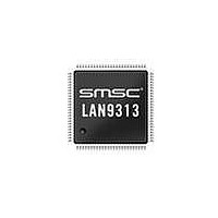
LAN9313I-NZW SMSC, LAN9313I-NZW Datasheet - Page 118

LAN9313I-NZW
Manufacturer Part Number
LAN9313I-NZW
Description
Ethernet ICs Three Port 10/100 Ethernet Switch
Manufacturer
SMSC
Type
Three Port Managed Ethernet Switchr
Datasheet
1.LAN9313-NZW.pdf
(399 pages)
Specifications of LAN9313I-NZW
Ethernet Connection Type
10 Base-T, 100 Base-TX
Minimum Operating Temperature
0 C
Mounting Style
SMD/SMT
Product
Ethernet Switches
Number Of Transceivers
1
Standard Supported
802.3, 802.3u
Data Rate
10 Mbps, 100 Mbps
Supply Voltage (max)
3.3 V
Supply Voltage (min)
0 V
Supply Current (max)
155 mA, 270 mA
Maximum Operating Temperature
+ 70 C
Package / Case
TQFP-100
Lead Free Status / RoHS Status
Lead free / RoHS Compliant
Available stocks
Company
Part Number
Manufacturer
Quantity
Price
Company:
Part Number:
LAN9313I-NZW
Manufacturer:
Standard
Quantity:
261
Company:
Part Number:
LAN9313I-NZW
Manufacturer:
Microchip Technology
Quantity:
10 000
- Current page: 118 of 399
- Download datasheet (5Mb)
Revision 1.7 (06-29-10)
8.3
8.4
MAC/PHY Modes
MAC/PHY Modes
MAC/PHY Modes
MAC/PHY Modes
SMI Managed
SPI Managed
I
Unmanaged
2
C Managed
MODE(S)
The SPI/I
LAN9313/LAN9313i. When in MAC/PHY I
MAC/PHY SPI managed modes, the SPI controller is enabled. The SPI/I
functionality and characteristics differ dependant on the selected modes as summarized in
Details on the various management modes and their configuration settings are provided in
"Modes of Operation," on page
When in MAC/PHY SPI managed mode, the SPI slave interface is used for CPU management of the
LAN9313/LAN9313i. All system CSRs are accessible to the CPU in these modes. SPI mode is
selected when the mngt_mode_strap[1:0] inputs are set to 11b. The SPI slave interface supports single
register and multiple register read and write commands. Multiple read and multiple write commands
support incrementing, decrementing, and static addressing.
Input data on the SI pin is sampled on the rising edge of the SCK input clock. Output data is sourced
on the SO pin with the falling edge of the clock. The SCK input clock can be either an active high
pulse or an active low pulse. When the nSCS chip select input is high, the SI input pin is ignored and
the SO output pin is three-stated.
A read or write command is started on the first rising edge of the input clock after nSCS goes low. An
8-bit instruction is then driven onto the line followed by an 8-bit register address field. All registers are
accessed as DWORDs. Appending two 0 bits to the address field will form the register address. This
is followed by one or more 32-bit data fields. All registers are accessed as DWORDs. All instructions,
addresses and data are transferred with the most-significant bit (msb) first. Data is transferred with the
most-significant byte (MSB) first (little endian).
The SPI interface supports up to a 10MHz input clock. A detailed SPI timing diagram is provided in
Section 14.5.5, "SPI Slave Timing," on page
SPI/I
SPI Slave Operation
2
C Slave Controller
Table 8.9 SPI / I
2
C slave controller functionality is dependant on the management mode of the
NOT USED
Input disabled
Output disabled
Pull-up enabled
SI
Input to SPI slave
Output disabled
Pull-up enabled
SDA
Input to I
Open-drain output
from I
Pull-up disabled
SI/SDA PIN
2
C slave
2
C slave
2
C Slave Serial Management Pins Characteristics
23.
DATASHEET
NOT USED
Output enabled
(driven low)
SO
Three-state output
from SPI slave
NOT USED
Output enabled
(driven low)
2
118
C managed modes, the I
SO PIN
392.
NOT USED
Input disabled
Pull-up enabled
nSCS
Input to SPI slave
Pull-up enabled
NOT USED
Input disabled
Pull-up enabled
Three Port 10/100 Managed Ethernet Switch with MII
nSCS PIN
2
C controller is enabled. When in
2
C serial management pins
SMSC LAN9313/LAN9313i
NOT USED
Input disabled
Pull-up enabled
SCK
Input to SPI slave
Pull-up enabled
SCL
Input to I
Pull-up disabled
SCK/SCL PIN
Section 2.3,
2
C slave
Table
Datasheet
8.9.
Related parts for LAN9313I-NZW
Image
Part Number
Description
Manufacturer
Datasheet
Request
R

Part Number:
Description:
Three Port 10/100 Managed Ethernet Switch with MII
Manufacturer:
SMSC [SMSC Corporation]
Datasheet:

Part Number:
Description:
Ethernet ICs Three Port 10/100 Ethernet Switch
Manufacturer:
SMSC
Datasheet:

Part Number:
Description:
Ethernet ICs Three Port 10/100 Ethernet Switch
Manufacturer:
SMSC
Datasheet:

Part Number:
Description:
FAST ETHERNET PHYSICAL LAYER DEVICE
Manufacturer:
SMSC Corporation
Datasheet:

Part Number:
Description:
357-036-542-201 CARDEDGE 36POS DL .156 BLK LOPRO
Manufacturer:
SMSC Corporation
Datasheet:

Part Number:
Description:
357-036-542-201 CARDEDGE 36POS DL .156 BLK LOPRO
Manufacturer:
SMSC Corporation
Datasheet:

Part Number:
Description:
357-036-542-201 CARDEDGE 36POS DL .156 BLK LOPRO
Manufacturer:
SMSC Corporation
Datasheet:

Part Number:
Description:
4-PORT USB2.0 HUB CONTROLLER
Manufacturer:
SMSC Corporation
Datasheet:

Part Number:
Description:
Manufacturer:
SMSC Corporation
Datasheet:

Part Number:
Description:
Manufacturer:
SMSC Corporation
Datasheet:

Part Number:
Description:
FDC37C672ENHANCED SUPER I/O CONTROLLER WITH FAST IR
Manufacturer:
SMSC Corporation
Datasheet:

Part Number:
Description:
COM90C66LJPARCNET Controller/Transceiver with AT Interface and On-Chip RAM
Manufacturer:
SMSC Corporation
Datasheet:

Part Number:
Description:
Manufacturer:
SMSC Corporation
Datasheet:

Part Number:
Description:
Manufacturer:
SMSC Corporation
Datasheet:


