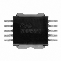
STV200N55F3 STMicroelectronics, STV200N55F3 Datasheet - Page 4

STV200N55F3
Manufacturer Part Number
STV200N55F3
Description
MOSFET N-CH 55V 200A POWERSO-10
Manufacturer
STMicroelectronics
Series
STripFET™r
Datasheet
1.STV200N55F3.pdf
(12 pages)
Specifications of STV200N55F3
Fet Type
MOSFET N-Channel, Metal Oxide
Fet Feature
Standard
Rds On (max) @ Id, Vgs
2.5 mOhm @ 75A, 10V
Drain To Source Voltage (vdss)
55V
Current - Continuous Drain (id) @ 25° C
200A
Vgs(th) (max) @ Id
4V @ 250µA
Gate Charge (qg) @ Vgs
100nC @ 10V
Input Capacitance (ciss) @ Vds
6800pF @ 25V
Power - Max
300W
Mounting Type
Surface Mount
Package / Case
PowerSO-10 Exposed Bottom Pad
Configuration
Single Quad Source
Transistor Polarity
N-Channel
Resistance Drain-source Rds (on)
1.8 Ohms
Drain-source Breakdown Voltage
55 V
Gate-source Breakdown Voltage
+/- 20 V
Continuous Drain Current
200 A
Power Dissipation
300 W
Maximum Operating Temperature
+ 175 C
Mounting Style
SMD/SMT
Minimum Operating Temperature
- 55 C
Lead Free Status / RoHS Status
Lead free / RoHS Compliant
Other names
497-7028-2
Electrical characteristics
2
4/12
Electrical characteristics
(T
Table 4.
Table 5.
V
Symbol
Symbol
case
R
V
(BR)DSS
I
C
I
C
DS(on)
C
Q
Q
GS(th)
GSS
DSS
Q
oss
rss
iss
gs
gd
g
= 25 °C unless otherwise specified)
Input capacitance
Output capacitance
Reverse transfer
capacitance
Total gate charge
Gate-source charge
Gate-drain charge
Drain-source
breakdown voltage
Zero gate voltage
drain current (V
Gate body leakage
current (V
Gate threshold voltage V
Static drain-source on
resistance
On /off states
Dynamic
Parameter
Parameter
DS
= 0)
GS
= 0)
V
V
V
Figure 14
I
V
V
V
V
D
GS
DS
DD
DS
DS
DS
DS
GS
= 250 µA, V
= 10 V
= Max rating,
= Max rating, T
= ± 20 V
= V
= 25 V, f = 1 MHz, V
= 44 V, I
= 10 V, I
Test conditions
Test conditions
GS
, I
D
D
D
= 250 µA
GS
= 75 A
= 120 A,
= 0
c
= 125 °C
GS
=0
Min.
Min.
55
2
6800
1450
Typ.
Typ.
100
1.8
15
30
26
STV200N55F3
Max.
±100
Max.
2.5
10
1
4
Unit
Unit
mΩ
µA
µA
nA
nC
nC
nC
pF
pF
pF
V
V


