IXTA3N120 IXYS, IXTA3N120 Datasheet - Page 2
IXTA3N120
Manufacturer Part Number
IXTA3N120
Description
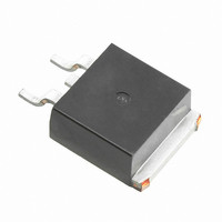
MOSFET N-CH 1.2KV 3A TO-263
Manufacturer
IXYS
Datasheet
1.IXTA3N120TRL.pdf
(4 pages)
Specifications of IXTA3N120
Fet Type
MOSFET N-Channel, Metal Oxide
Fet Feature
Standard
Rds On (max) @ Id, Vgs
4.5 Ohm @ 500mA, 10V
Drain To Source Voltage (vdss)
1200V (1.2kV)
Current - Continuous Drain (id) @ 25° C
3A
Vgs(th) (max) @ Id
5V @ 250µA
Gate Charge (qg) @ Vgs
42nC @ 10V
Input Capacitance (ciss) @ Vds
1350pF @ 25V
Power - Max
200W
Mounting Type
Surface Mount
Package / Case
D²Pak, TO-263 (2 leads + tab)
Configuration
Single
Transistor Polarity
N-Channel
Resistance Drain-source Rds (on)
4.5 Ohms
Forward Transconductance Gfs (max / Min)
2.6 s
Drain-source Breakdown Voltage
1100 V
Gate-source Breakdown Voltage
+/- 20 V
Continuous Drain Current
3 A
Power Dissipation
150 W
Maximum Operating Temperature
+ 150 C
Mounting Style
SMD/SMT
Minimum Operating Temperature
- 55 C
Vdss, Max, (v)
1200
Id(cont), Tc=25°c, (a)
3
Rds(on), Max, Tj=25°c, (?)
4.5
Ciss, Typ, (pf)
1050
Qg, Typ, (nc)
39
Trr, Typ, (ns)
700
Pd, (w)
200
Rthjc, Max, (k/w)
0.62
Package Style
TO-263
Lead Free Status / RoHS Status
Lead free / RoHS Compliant
Other names
Q2023873
Available stocks
Company
Part Number
Manufacturer
Quantity
Price
Company:

Part Number:
IXTA3N120
Manufacturer:
IXYS
Quantity:
18 000
Part Number:
IXTA3N120
Manufacturer:
IXYS/艾赛斯
Quantity:
20 000


IXYS reserves the right to change limits, test conditions, and dimensions.
Symbol
g
C
C
C
t
t
t
t
Q
Q
Q
R
R
Source-Drain Diode
Symbol
I
I
V
t
Notes: 1. Pulse test, t ≤ 300 µs, duty cycle d ≤ 2 %
IXYS MOSFETs and IGBTs are covered by one or more
of the following U.S. patents:
d(on)
d(off)
f
S
SM
r
rr
fs
thJC
thCK
SD
iss
oss
rss
g(on)
gd
gs
Test Conditions
V
Test Conditions
V
Repetitive; pulse width limited by T
I
I
F
F
DS
GS
= I
= I
S
S
= 0 V
= 20 V; I
V
V
R
V
(TO-220)
, V
, -di/dt = 100 A/µs, V
GS
GS
GS
G
= 4.7 Ω (External),
GS
= 0 V, V
= 10 V, V
= 10 V, V
= 0 V, Note 1
D
= 0.5 • I
DS
DS
DS
= 25 V, f = 1 MHz
= 0.5 • V
= 0.5 • V
D25
, Note 1
R
= 100 V
(T
(T
DSS
DSS
J
J
= 25°C, unless otherwise specified)
, I
, I
= 25°C, unless otherwise specified)
4,835,592 4,881,106 5,017,508 5,049,961 5,187,117 5,486,715 6,306,728B1 6,259,123B1 6,306,728B1
4,850,072 4,931,844 5,034,796 5,063,307 5,237,481 5,381,025 6,404,065B1 6,162,665
D
D
JM
= 0.5 • I
= 0.5 • I
D25
D25
min.
min.
1.5
Characteristic Values
Characteristic Values
1100 1350
0.25
typ.
typ.
700
110 135
2.6
40
17
15
32
18
42
21
8
0.62
max.
max.
60
1.5
12
3
K/W
K/W
nC
nC
nC
pF
pF
pF
n s
n s
n s
n s
n s
S
A
A
V
Pins: 1 - Gate
Dim.
A
A1
b
b2
c
c2
D
D1
E
E1
e
L
L1
L2
L3
L4
R
TO-263 (IXTA) Outline
TO-220 (IXTP) Outline
3 - Source
14.61
Min.
4.06
2.03
0.51
1.14
0.46
1.14
8.64
7.11
9.65
6.86
2.54
2.29
1.02
1.27
0.46
Millimeter
0
IXTA 3N120
IXTP 3N120
10.29
15.88
Max.
BSC
4.83
2.79
0.99
1.40
0.74
1.40
9.65
8.13
8.13
2.79
1.40
1.78
0.38
0.74
2 - Drain
4 - Drain
Bottom Side
Min.
.160
.080
.020
.045
.018
.045
.340
.280
.380
.270
.100
.575
.090
.040
.050
.018
1. Gate
2. Drain
3. Source
4. Drain
Inches
0
Bottom Side
6,534,343
Max.
BSC
.190
.110
.039
.055
.029
.055
.380
.320
.405
.320
.625
.110
.055
.070
.015
.029
Related parts for IXTA3N120
Image
Part Number
Description
Manufacturer
Datasheet
Request
R


Part Number:
Description:
HiPerFET Power MOSFETs
Manufacturer:
IXYS Corporation
Datasheet:
Part Number:
Description:
J-K-Type Flip-Flop
Manufacturer:
IXYS Corporation
Datasheet:
Part Number:
Description:
HiPerRF Power MOSFETs
Manufacturer:
IXYS Corporation
Datasheet:
Part Number:
Description:
Rectifier Module for Three Phase Power Factor Correction
Manufacturer:
IXYS Corporation
Datasheet:
Part Number:
Description:
Thyristor Modules Thyristor/Diode Modules
Manufacturer:
IXYS Corporation
Datasheet:
Part Number:
Description:
Thyristor Modules Thyristor/Diode Modules
Manufacturer:
IXYS Corporation
Datasheet:
Part Number:
Description:
Thyristor Modules Thyristor/Diode Modules
Manufacturer:
IXYS Corporation
Datasheet:
Part Number:
Description:
Thyristor Modules Thyristor/Diode Modules
Manufacturer:
IXYS Corporation
Datasheet:
Part Number:
Description:
Thyristor Modules /Diode Modules
Manufacturer:
IXYS Corporation
Datasheet: