STW11NK100Z STMicroelectronics, STW11NK100Z Datasheet - Page 3
STW11NK100Z
Manufacturer Part Number
STW11NK100Z
Description
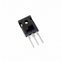
MOSFET N-CH 1KV 8.3A TO-247
Manufacturer
STMicroelectronics
Series
SuperMESH™r
Datasheet
1.STW11NK100Z.pdf
(14 pages)
Specifications of STW11NK100Z
Fet Type
MOSFET N-Channel, Metal Oxide
Fet Feature
Standard
Rds On (max) @ Id, Vgs
1.38 Ohm @ 4.15A, 10V
Drain To Source Voltage (vdss)
1000V (1kV)
Current - Continuous Drain (id) @ 25° C
8.3A
Vgs(th) (max) @ Id
4.5V @ 100µA
Gate Charge (qg) @ Vgs
162nC @ 10V
Input Capacitance (ciss) @ Vds
3500pF @ 25V
Power - Max
230W
Mounting Type
Through Hole
Package / Case
TO-247-3
Configuration
Single
Transistor Polarity
N-Channel
Resistance Drain-source Rds (on)
1.38 Ohm @ 10 V
Drain-source Breakdown Voltage
1000 V
Gate-source Breakdown Voltage
+/- 30 V
Continuous Drain Current
8.3 A
Power Dissipation
230000 mW
Maximum Operating Temperature
+ 150 C
Mounting Style
Through Hole
Minimum Operating Temperature
- 55 C
Lead Free Status / RoHS Status
Lead free / RoHS Compliant
Other names
497-3255-5
Available stocks
Company
Part Number
Manufacturer
Quantity
Price
Company:

Part Number:
STW11NK100Z
Manufacturer:
ST
Quantity:
12 500


STW11NK100Z
1
Electrical ratings
Table 1.
1. Pulse width limited by safe operating area
2. I
Table 2.
Table 3.
Symbol
R
Symbol
V
R
Symbol
thj-case
ESD (G-S)
dv/dt
SD
E
I
V
I
thj-a
AR
P
T
DM
AS
V
V
T
DGR
l
T
I
I
TOT
≤ 8.3 A, di/dt ≤ 200A/µs, V
DS
GS
stg
D
D
J
(1)
(2)
Thermal resistance junction-case Max
Thermal resistance junction-ambient Max
Maximum lead temperature for soldering
purpose
Avalanche current, repetitive or not-repetitive
(pulse width limited by Tj Max)
Single pulse avalanche energy
(starting Tj=25°C, Id=Iar, Vdd=50V)
Absolute maximum ratings
Thermal data
Avalanche characteristics
Drain-source voltage (V
Drain-gate voltage (R
Gate-source voltage
Drain current (continuous) at T
Drain current (continuous) at T
Drain current (pulsed)
Total dissipation at T
Derating Factor
Gate source ESD(HBM-C=100pF, R=1,5KΩ)
Peak diode recovery voltage slope
Operating junction temperature
Storage temperature
DD
Parameter
≤ V
(BR)DSS
Parameter
Parameter
C
GS
= 25°C
GS
= 20KΩ)
, T
= 0)
j
≤ T
JMAX
C
C
=100°C
= 25°C
Value
0.54
300
50
-55 to 150
Value
Value
1000
1000
6000
550
± 30
33.2
1.85
8.3
230
8.3
5.2
4.5
Electrical ratings
°C/W
°C/W
W/°C
Unit
Unit
Unit
V/ns
mJ
°C
°C
W
A
V
V
V
A
A
A
V
3/14
Related parts for STW11NK100Z
Image
Part Number
Description
Manufacturer
Datasheet
Request
R

Part Number:
Description:
STMicroelectronics [RIPPLE-CARRY BINARY COUNTER/DIVIDERS]
Manufacturer:
STMicroelectronics
Datasheet:
Part Number:
Description:
STMicroelectronics [LIQUID-CRYSTAL DISPLAY DRIVERS]
Manufacturer:
STMicroelectronics
Datasheet:

Part Number:
Description:
BOARD EVAL FOR MEMS SENSORS
Manufacturer:
STMicroelectronics
Datasheet:
Part Number:
Description:
NPN TRANSISTOR POWER MODULE
Manufacturer:
STMicroelectronics
Datasheet:
Part Number:
Description:
TURBOSWITCH ULTRA-FAST HIGH VOLTAGE DIODE
Manufacturer:
STMicroelectronics
Datasheet:
Part Number:
Description:
Manufacturer:
STMicroelectronics
Datasheet:
Part Number:
Description:
DIODE / SCR MODULE
Manufacturer:
STMicroelectronics
Datasheet:
Part Number:
Description:
DIODE / SCR MODULE
Manufacturer:
STMicroelectronics
Datasheet:
Part Number:
Description:
Search -----> STE16N100
Manufacturer:
STMicroelectronics
Datasheet:
Part Number:
Description:
Search ---> STE53NA50
Manufacturer:
STMicroelectronics
Datasheet:
Part Number:
Description:
NPN Transistor Power Module
Manufacturer:
STMicroelectronics
Datasheet:
Part Number:
Description:
DIODE / SCR MODULE
Manufacturer:
STMicroelectronics
Datasheet: