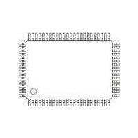
PCA9620H/Q900/1,51 NXP Semiconductors, PCA9620H/Q900/1,51 Datasheet - Page 54

PCA9620H/Q900/1,51
Manufacturer Part Number
PCA9620H/Q900/1,51
Description
LCD Drivers 480 SEGMENT LCD SEGMENT DRIVER
Manufacturer
NXP Semiconductors
Datasheet
1.PCA9620HQ900151.pdf
(71 pages)
Specifications of PCA9620H/Q900/1,51
Number Of Segments
60
Maximum Clock Frequency
14500 Hz
Operating Supply Voltage
2.5 V to 5.5 V
Maximum Power Dissipation
400 mW
Maximum Operating Temperature
+ 105 C
Package / Case
LQFP-80
Maximum Supply Current
200 uA
Minimum Operating Temperature
- 40 C
Lead Free Status / RoHS Status
Lead free / RoHS Compliant
Other names
935291899518
Available stocks
Company
Part Number
Manufacturer
Quantity
Price
Company:
Part Number:
PCA9620H/Q900/1,51
Manufacturer:
NXP Semiconductors
Quantity:
10 000
NXP Semiconductors
10. Limiting values
PCA9620
Product data sheet
CAUTION
Table 34.
In accordance with the Absolute Maximum Rating System (IEC 60134).
[1]
[2]
[3]
[4]
Symbol
V
V
I
I
V
I
V
I
V
I
P
P/out
V
I
T
T
I
DD1
DD2
DD(LCD)
I
O
SS
lu
stg
amb
DD1
DD2
LCD
i
O
tot
ESD
Pass level; Human Body Model (HBM), according to
Pass level; Charged-Device Model (CDM), according to
Pass level; latch-up testing according to
According to the NXP store and transport requirements (see
stored at a temperature of +8 °C to +45 °C and a humidity of 25 % to 75 %. For long term storage products
divergent conditions are described in that document.
Static voltages across the liquid crystal display can build up when the LCD supply voltage
(V
display artifacts. To avoid such artifacts, V
LCD
) is on while the IC supply voltage (V
Limiting values
Parameter
supply voltage 1
supply voltage 2
supply current 1
supply current 2
LCD supply voltage
LCD supply current
input voltage
input current
output voltage
output current
ground supply current
total power dissipation
power dissipation per
output
electrostatic discharge
voltage
latch-up current
storage temperature
ambient temperature
All information provided in this document is subject to legal disclaimers.
Rev. 1 — 9 December 2010
Ref. 8 “JESD78”
Conditions
analog and digital
charge pump
analog and digital
charge pump
on pins CLK,
SDA, SCL, A0,
A1, T1, T2, T3
on pins S0 to S59,
BP0 to BP7
on pins SDA, CLK
HBM
CDM
operating device
Universal LCD driver for low multiplex rates
LCD
DD
) is off, or vice versa. This may cause unwanted
and V
Ref. 6
Ref. 7
at maximum ambient temperature (T
DD
“JESD22-A114”.
Ref. 10
must be applied or removed together.
“JESD22-C101”.
[1]
[2]
[3]
[4]
“NX3-00092”) the devices have to be
Min
−0.5
−0.5
−50
−50
−0.5
−50
−0.5
−10
−0.5
−0.5
−10
−50
-
-
-
-
-
−65
−40
PCA9620
© NXP B.V. 2010. All rights reserved.
Max
+6.5
+6.5
+50
+50
+10
+50
+6.5
+10
+10
+6.5
+10
+50
400
100
±4000
±1500
100
+150
+105
amb(max)
V
V
Unit
V
V
mA
mA
mA
V
mA
V
mA
mA
mW
mW
V
V
mA
°C
°C
54 of 71
).


