SUM110N04-03P-E3 Vishay, SUM110N04-03P-E3 Datasheet - Page 2
SUM110N04-03P-E3
Manufacturer Part Number
SUM110N04-03P-E3
Description
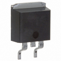
MOSFET N-CH 40V 110A D2PAK
Manufacturer
Vishay
Series
TrenchFET®r
Datasheet
1.SUM110N04-03P-E3.pdf
(6 pages)
Specifications of SUM110N04-03P-E3
Fet Type
MOSFET N-Channel, Metal Oxide
Fet Feature
Standard
Rds On (max) @ Id, Vgs
3.1 mOhm @ 30A, 10V
Drain To Source Voltage (vdss)
40V
Current - Continuous Drain (id) @ 25° C
110A
Vgs(th) (max) @ Id
4V @ 250µA
Gate Charge (qg) @ Vgs
150nC @ 10V
Input Capacitance (ciss) @ Vds
6500pF @ 25V
Power - Max
3.75W
Mounting Type
Surface Mount
Package / Case
D²Pak, TO-263 (2 leads + tab)
Lead Free Status / RoHS Status
Lead free / RoHS Compliant
Other names
SUM110N04-03P-E3
SUM110N04-03P-E3TR
SUM110N04-03P-E3TR


SUM110N04-03P
Vishay Siliconix
Notes:
a. Pulse test; pulse width ≤ 300 µs, duty cycle ≤ 2 %.
b. Guaranteed by design, not subject to production testing.
c. Independent of operating temperature.
Stresses beyond those listed under “Absolute Maximum Ratings” may cause permanent damage to the device. These are stress ratings only, and functional operation
of the device at these or any other conditions beyond those indicated in the operational sections of the specifications is not implied. Exposure to absolute maximum
rating conditions for extended periods may affect device reliability.
www.vishay.com
2
SPECIFICATIONS T
Parameter
Static
Drain-Source Breakdown Voltage
Gate-Threshold Voltage
Gate-Body Leakage
Zero Gate Voltage Drain Current
On-State Drain Current
Drain-Source On-State Resistance
Forward Transconductance
Dynamic
Input Capacitance
Output Capacitance
Reverse Transfer Capacitance
Total Gate Charge
Gate-Source Charge
Gate-Drain Charge
Gate Resistance
Turn-On Delay Time
Rise Time
Turn-Off Delay Time
Fall Time
Source-Drain Diode Ratings and Characteristics T
Continuous Current
Pulsed Current
Forward Voltage
Reverse Recovery Time
Peak Reverse Recovery Charge
Reverse Recovery Charge
c
b
c
a
c
c
c
c
c
a
a
J
= 25 °C, unless otherwise noted
a
V
I
Symbol
RM(REC)
V
r
(BR)DSS
I
DS(on)
t
t
I
C
I
C
V
GS(th)
D(on)
C
Q
Q
d(on)
d(off)
GSS
DSS
I
Q
Q
g
R
SM
I
t
oss
t
t
rss
SD
iss
S
rr
fs
gs
gd
r
f
g
rr
g
C
= 25 °C
I
D
V
V
V
V
V
V
DS
DS
DS
GS
GS
≅ 110 A, V
GS
I
= 40 V, V
= 40 V, V
= 30 V, V
= 10 V, I
= 10 V, I
F
V
V
V
= 0 V, V
V
V
V
V
DD
b
= 85 A, di/dt = 100 A/µs
DS
V
DS
I
DS
DS
F
DS
DS
GS
Test Conditions
= 85 A, V
= 0 V, V
= 30 V, R
= V
= 0 V, I
= 40 V, V
≥ 5 V, V
= 10 V, I
= 15 V, I
GEN
f = 1 MHz
D
D
GS
DS
GS
GS
GS
= 30 A, T
= 30 A, T
, I
= 25 V, f = 1 MHz
= 0 V, T
= 0 V, T
= 10 V, I
= 10 V, R
D
GS
D
GS
GS
L
= 250 µA
D
D
GS
= 250 µA
= 0.27 Ω
= ± 20 V
= 30 A
= 30 A
= 10 V
= 0 V
= 0 V
J
J
J
J
D
= 125 °C
= 175 °C
= 125 °C
= 175 °C
G
= 110 A
= 2.5 Ω
Min.
120
2.5
0.5
40
30
0.0025
0.075
6500
1400
Typ.
570
145
1.1
1.1
2.5
90
35
22
35
20
55
60
S-80274-Rev. C, 11-Feb-08
Document Number: 72346
0.0031
0.0049
0.0059
Max.
0.22
100
250
150
220
110
240
1.9
1.5
50
55
30
85
90
4
1
5
Unit
nA
µA
pF
nC
µC
ns
ns
Ω
Ω
V
A
S
A
V
A
Related parts for SUM110N04-03P-E3
Image
Part Number
Description
Manufacturer
Datasheet
Request
R

Part Number:
Description:
MOSFET N-CH 40V 110A D2PAK
Manufacturer:
Vishay
Datasheet:
Part Number:
Description:
TRANSISTOR,MOSFET,N-CHANNEL,40V V(BR)DSS,110A I(D),TO-263AB
Manufacturer:
Vishay
Datasheet:
Part Number:
Description:
MOSFET N-CH 40V 110A D2PAK
Manufacturer:
Vishay
Datasheet:

Part Number:
Description:
N-Channel 40-V (D-S) 175 �C MOSFET
Manufacturer:
VISHAY [Vishay Siliconix]
Datasheet:

Part Number:
Description:
N CHANNEL MOSFET, 40V, 11A, TO-263
Manufacturer:
Vishay
Datasheet:

Part Number:
Description:
N CHANNEL MOSFET, 40V, 85A
Manufacturer:
Vishay
Datasheet:
Part Number:
Description:
N CHANNEL MOSFET, 40V, 85A
Manufacturer:
Vishay
Datasheet:
Part Number:
Description:
N CHANNEL MOSFET, 40V, 110A
Manufacturer:
Vishay
Datasheet:

Part Number:
Description:
TRANSISTOR,MOSFET,N-CHANNEL,40V V(BR)DSS,110A I(D),TO-263AB
Manufacturer:
Vishay
Part Number:
Description:
N-Channel 40-V (D-S) 200C MOSFET
Manufacturer:
Vishay Siliconix
Datasheet:
Part Number:
Description:
N-Channel 40-V (D-S) 175C MOSFET
Manufacturer:
Vishay Siliconix
Datasheet:
Part Number:
Description:
N-Channel MOSFET
Manufacturer:
Vishay Siliconix
Datasheet:
Part Number:
Description:
N-Channel 40-V (D-S) 175C MOSFET
Manufacturer:
Vishay Siliconix
Datasheet:
Part Number:
Description:
N-channel 40-v 175c Mosfet
Manufacturer:
Vishay
Datasheet:
Part Number:
Description:
N-channel 40-v D-s Mosfet
Manufacturer:
Vishay
Datasheet: