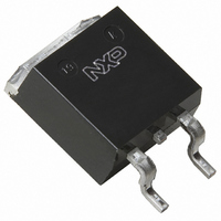
BUK9610-55A,118 NXP Semiconductors, BUK9610-55A,118 Datasheet - Page 8

BUK9610-55A,118
Manufacturer Part Number
BUK9610-55A,118
Description
MOSFET N-CH 55V 75A SOT404
Manufacturer
NXP Semiconductors
Series
TrenchMOS™r
Specifications of BUK9610-55A,118
Package / Case
D²Pak, TO-263 (2 leads + tab)
Fet Type
MOSFET N-Channel, Metal Oxide
Fet Feature
Logic Level Gate
Rds On (max) @ Id, Vgs
9 mOhm @ 25A, 10V
Drain To Source Voltage (vdss)
55V
Current - Continuous Drain (id) @ 25° C
75A
Vgs(th) (max) @ Id
2V @ 1mA
Gate Charge (qg) @ Vgs
68nC @ 5V
Input Capacitance (ciss) @ Vds
4307pF @ 25V
Power - Max
200W
Mounting Type
Surface Mount
Minimum Operating Temperature
- 55 C
Configuration
Single
Transistor Polarity
N-Channel
Resistance Drain-source Rds (on)
0.009 Ohm @ 10 V
Drain-source Breakdown Voltage
55 V
Gate-source Breakdown Voltage
+/- 15 V
Continuous Drain Current
75 A
Power Dissipation
200000 mW
Maximum Operating Temperature
+ 175 C
Mounting Style
SMD/SMT
Fall Time
139 ns
Rise Time
155 ns
Lead Free Status / RoHS Status
Lead free / RoHS Compliant
Lead Free Status / RoHS Status
Lead free / RoHS Compliant, Lead free / RoHS Compliant
Other names
934056852118
BUK9610-55A /T3
BUK9610-55A /T3
BUK9610-55A /T3
BUK9610-55A /T3
NXP Semiconductors
BUK9610-55A
Product data sheet
Fig 13. Gate-source voltage as a function of gate
Fig 15. Reverse diode current as a function of reverse diode voltage; typical values
V
(V)
GS
5
4
3
2
1
0
charge; typical values
0
20
V
DD
= 14 V
40
V
DD
= 44 V
(A)
I
S
100
80
60
40
20
0
60
0
All information provided in this document is subject to legal disclaimers.
Q
G
(nC)
03nd71
Rev. 02 — 16 February 2011
80
0.5
T
j
= 175 °C
Fig 14. Input, output and reverse transfer capacitances
(pF)
1.0
8000
6000
4000
2000
C
0
10
as a function of drain-source voltage; typical
values
T
V
j
SD
−2
= 25 °C
(V)
03nd70
N-channel TrenchMOS logic level FET
1.5
10
−1
BUK9610-55A
C
1
C
C
rss
iss
oss
10
© NXP B.V. 2011. All rights reserved.
V
DS
03nd77
(V)
10
2
8 of 13


