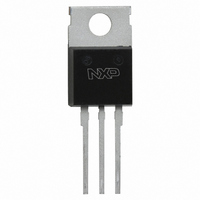
BUK7515-100A,127 NXP Semiconductors, BUK7515-100A,127 Datasheet - Page 2

BUK7515-100A,127
Manufacturer Part Number
BUK7515-100A,127
Description
MOSFET N-CH 100V 75A SOT78
Manufacturer
NXP Semiconductors
Series
TrenchMOS™r
Specifications of BUK7515-100A,127
Package / Case
TO-220AB-3
Fet Type
MOSFET N-Channel, Metal Oxide
Fet Feature
Standard
Rds On (max) @ Id, Vgs
15 mOhm @ 25A, 10V
Drain To Source Voltage (vdss)
100V
Current - Continuous Drain (id) @ 25° C
75A
Vgs(th) (max) @ Id
4V @ 1mA
Input Capacitance (ciss) @ Vds
6000pF @ 25V
Power - Max
300W
Mounting Type
Through Hole
Minimum Operating Temperature
- 55 C
Configuration
Single
Transistor Polarity
N-Channel
Resistance Drain-source Rds (on)
0.15 Ohm @ 10 V
Drain-source Breakdown Voltage
100 V
Gate-source Breakdown Voltage
+/- 20 V
Continuous Drain Current
75 A
Power Dissipation
300000 mW
Maximum Operating Temperature
+ 175 C
Mounting Style
SMD/SMT
Lead Free Status / RoHS Status
Lead free / RoHS Compliant
Gate Charge (qg) @ Vgs
-
Lead Free Status / Rohs Status
Lead free / RoHS Compliant
Other names
934055409127
BUK7515-100A
BUK7515-100A
BUK7515-100A
BUK7515-100A
Philips Semiconductors
STATIC CHARACTERISTICS
T
DYNAMIC CHARACTERISTICS
T
REVERSE DIODE LIMITING VALUES AND CHARACTERISTICS
T
AVALANCHE LIMITING VALUE
June 2003
TrenchMOS
Standard level FET
j
SYMBOL PARAMETER
V
V
I
I
R
mb
SYMBOL PARAMETER
C
C
C
t
t
t
t
L
L
L
j
SYMBOL PARAMETER
I
I
V
t
Q
SYMBOL PARAMETER
W
= 25˚C unless otherwise specified
DSS
GSS
d on
r
d off
f
DR
DRM
rr
= 25˚C unless otherwise specified
d
d
s
(BR)DSS
GS(TO)
SD
DS(ON)
iss
oss
rss
rr
DSS
= 25˚C unless otherwise specified
Drain-source breakdown
voltage
Gate threshold voltage
Zero gate voltage drain current
Gate source leakage current
Drain-source on-state
resistance
Input capacitance
Output capacitance
Feedback capacitance
Turn-on delay time
Turn-on rise time
Turn-off delay time
Turn-off fall time
Internal drain inductance
Internal drain inductance
Internal source inductance
Continuous reverse drain
current
Pulsed reverse drain current
Diode forward voltage
Reverse recovery time
Reverse recovery charge
Drain-source non-repetitive
unclamped inductive turn-off
energy
transistor
CONDITIONS
V
V
V
V
V
CONDITIONS
V
V
V
Measured from contact screw on
tab to centre of die
Measured from drain lead 6 mm
from package to centre of die
Measured from source lead 6 mm
from package to source bond pad
CONDITIONS
I
I
I
V
CONDITIONS
I
V
F
F
F
D
GS
DS
DS
GS
GS
GS
DD
GS
GS
GS
= 25 A; V
= 75 A; V
= 75 A; -dI
= 35 A; V
= V
= 100 V; V
= 0 V; I
= 20 V; V
= 10 V; I
= 0 V; V
= 30 V; R
= 10 V; R
= -10 V; V
= 10 V; R
GS
; I
2
D
D
GS
GS
DD
DS
D
F
= 0.25 mA;
= 1 mA
/dt = 100 A/ s;
load
G
GS
= 0 V
= 0 V
= 25 A
R
GS
DS
= 25 V; f = 1 MHz
= 10
= 30 V
25 V;
= 50 ; T
=1.2 ;
= 0 V;
= 0 V
T
T
T
T
T
j
j
j
mb
j
j
= 175˚C
= 175˚C
= 175˚C
= -55˚C
= -55˚C
= 25 ˚C
MIN.
MIN.
MIN.
MIN.
100
89
2
1
-
-
-
-
-
-
-
-
-
-
-
-
-
-
-
-
-
-
-
-
-
-
-
TYP.
TYP.
4500
TYP.
TYP.
0.05
12.0
0.85
0.35
550
305
150
3.0
3.5
4.5
7.5
1.1
BUK7515-100A
35
85
70
80
2
-
-
-
-
-
-
-
-
-
Product specification
MAX.
MAX.
MAX.
MAX.
6000
15.0
40.5
500
100
660
400
125
225
100
240
120
4.0
4.4
1.2
10
55
75
-
-
-
-
-
-
-
-
-
Rev 1.200
UNIT
UNIT
UNIT
UNIT
m
m
nH
nH
nH
mJ
nA
pF
pF
pF
ns
ns
ns
ns
ns
V
V
V
V
V
A
A
V
V
C
A
A


