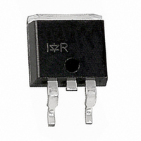
IRF540NSTRRPBF International Rectifier, IRF540NSTRRPBF Datasheet - Page 4

IRF540NSTRRPBF
Manufacturer Part Number
IRF540NSTRRPBF
Description
MOSFET N-CH 100V 33A D2PAK
Manufacturer
International Rectifier
Series
HEXFET®r
Type
Power MOSFETr
Datasheet
1.IRF540NSTRLPBF.pdf
(11 pages)
Specifications of IRF540NSTRRPBF
Fet Type
MOSFET N-Channel, Metal Oxide
Fet Feature
Standard
Rds On (max) @ Id, Vgs
44 mOhm @ 16A, 10V
Drain To Source Voltage (vdss)
100V
Current - Continuous Drain (id) @ 25° C
33A
Vgs(th) (max) @ Id
4V @ 250µA
Gate Charge (qg) @ Vgs
71nC @ 10V
Input Capacitance (ciss) @ Vds
1960pF @ 25V
Power - Max
130W
Mounting Type
Surface Mount
Package / Case
D²Pak, TO-263 (2 leads + tab)
Number Of Elements
1
Polarity
N
Channel Mode
Enhancement
Drain-source On-res
0.044Ohm
Drain-source On-volt
100V
Gate-source Voltage (max)
±20V
Drain Current (max)
33A
Power Dissipation
130W
Output Power (max)
Not RequiredW
Frequency (max)
Not RequiredMHz
Noise Figure
Not RequireddB
Power Gain
Not RequireddB
Drain Efficiency
Not Required%
Operating Temp Range
-55C to 175C
Operating Temperature Classification
Military
Mounting
Surface Mount
Pin Count
2 +Tab
Package Type
D2PAK
Configuration
Single
Transistor Polarity
N-Channel
Resistance Drain-source Rds (on)
44 m Ohms
Drain-source Breakdown Voltage
100 V
Gate-source Breakdown Voltage
20 V
Continuous Drain Current
33 A
Maximum Operating Temperature
+ 175 C
Mounting Style
SMD/SMT
Fall Time
35 ns
Gate Charge Qg
47.3 nC
Minimum Operating Temperature
- 55 C
Rise Time
35 ns
Lead Free Status / RoHS Status
Lead free / RoHS Compliant
4
3000
2500
2000
1500
1000
500
1000
100
0.1
0
10
Fig 5. Typical Capacitance Vs.
1
Fig 7. Typical Source-Drain Diode
1
0.2
Drain-to-Source Voltage
T = 175 C
V
J
V
DS
SD
Forward Voltage
V
C
C
C
, Drain-to-Source Voltage (V)
0.6
GS
iss
rss
oss
,Source-to-Drain Voltage (V)
°
=
=
=
=
0V,
C
C
C
C oss
C rss
C iss
gs
gd
ds
+ C
+ C
10
1.0
T = 25 C
f = 1MHz
gd ,
gd
J
C
°
ds
1.4
SHORTED
V
GS
= 0 V
100
1.8
1000
100
0.1
10
1
20
16
12
8
4
0
1
0
Fig 8. Maximum Safe Operating Area
I =
Fig 6. Typical Gate Charge Vs.
D
T A = 25°C
T J = 175°C
Single Pulse
16A
V DS , Drain-toSource Voltage (V)
Gate-to-Source Voltage
Q , Total Gate Charge (nC)
G
20
10
OPERATION IN THIS AREA
LIMITED BY R DS (on)
V
V
V
40
DS
DS
DS
= 80V
= 50V
= 20V
FOR TEST CIRCUIT
SEE FIGURE
100
www.irf.com
100µsec
60
1msec
10msec
13
1000
80


