STW26NM60 STMicroelectronics, STW26NM60 Datasheet
STW26NM60
Specifications of STW26NM60
Available stocks


Related parts for STW26NM60


STW26NM60 Summary of contents
Page 1
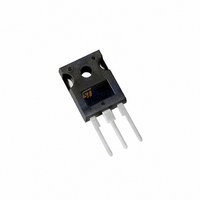
... Table 2: Order Codes SALES TYPE STW26NM60 February 2005 N-CHANNEL 600V - 0.125 - 30A TO-247 Figure 1: Package R I DS(on) D < 0.135 30 A product has an Figure 2: Internal Schematic Diagram MARKING PACKAGE W26NM60 TO-247 STW26NM60 MDmesh™ MOSFET TO-247 PACKAGING TUBE Rev. 5 1/9 ...
Page 2
... STW26NM60 Table 3: Absolute Maximum ratings Symbol V Drain-source Voltage ( Drain-gate Voltage (R DGR V Gate- source Voltage GS I Drain Current (continuous Drain Current (continuous Drain Current (pulsed Total Dissipation at T TOT Derating Factor V Gate source ESD(HBM-C=100pF, R=1.5K ESD(G-S) dv/dt (1) Peak Diode Recovery voltage slope ...
Page 3
... (see Figure 18) Test Conditions di/dt = 100 A/µ 100V DD (see Figure 16 di/dt = 100 A/µ 100V 150° (see Figure 16) STW26NM60 Min. Typ. Max. Unit 600 V 10 µA 100 µA ± 10 µ 0.125 0.135 Min. Typ. Max. Unit 20 S 2900 pF 900 pF 40 ...
Page 4
... STW26NM60 Figure 3: Safe Operating Area Figure 4: Output Characteristics Figure 5: Transconductance 4/9 Figure 6: Thermal Impedance Figure 7: Transfer Characteristics Figure 8: Static Drain-source On Resistance ...
Page 5
... Figure 9: Gate Charge vs Gate-source Voltage Figure 10: Normalized Gate Thereshold Volt- age vs Temperature Figure 11: Dource-Drain Diode Forward Char- acteristics Figure 12: Capacitance Variations Figure 13: Normalized On Resistance vs Tem- perature STW26NM60 5/9 ...
Page 6
... STW26NM60 Figure 14: Unclamped Inductive Load Test Cir- cuit Figure 15: Switching Times Test Circuit For Resistive Load Figure 16: Test Circuit For Inductive Load Switching and Diode Recovery Times 6/9 Figure 17: Unclamped Inductive Wafeform Figure 18: Gate Charge Test Circuit ...
Page 7
... STW26NM60 MAX. 0.20 0.102 0.055 0.094 0.134 0.03 0.793 0.620 0.582 0.17 0.143 0.216 7/9 ...
Page 8
... STW26NM60 Table 10: Revision History Date Revision 24-June-2004 4 04-Feb-2004 5 8/9 Description of Changes New Stylesheet. No Content Change New Id current on title in first page ...
Page 9
... All other names are the property of their respective owners Australia - Belgium - Brazil - Canada - China - Czech Republic - Finland - France - Germany - Hong Kong - India - Israel - Italy - Japan - Malaysia - Malta - Morocco - Singapore - Spain - Sweden - Switzerland - United Kingdom - United States of America © 2005 STMicroelectronics - All Rights Reserved STMicroelectronics group of companies STW26NM60 9/9 ...