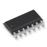
UBA2021T/N2 NXP Semiconductors, UBA2021T/N2 Datasheet - Page 9

UBA2021T/N2
Manufacturer Part Number
UBA2021T/N2
Description
CFL Lamp DRVR 14-Pin SO Tube
Manufacturer
NXP Semiconductors
Datasheet
1.UBA2021PN2112.pdf
(16 pages)
Specifications of UBA2021T/N2
Package
14SO
Driver Type
CFL Lamp
Module Configuration
Half Bridge
Supply Current
1mA
Meter Display Type
Fluorescent Lamp
Supply Voltage Range
9.55V To 10.75V, 11.35V To 12.55V
Driver Case Style
SOIC
No. Of Pins
14
Operating
RoHS Compliant
Operating Supply Voltage
630 V
Maximum Operating Temperature
+ 150 C
Mounting Style
SMD/SMT
Package / Case
SOIC-14
Minimum Operating Temperature
- 40 C
Lead Free Status / Rohs Status
Details
Available stocks
Company
Part Number
Manufacturer
Quantity
Price
Part Number:
UBA2021T/N2
Manufacturer:
NXP/恩智浦
Quantity:
20 000
Company:
Part Number:
UBA2021T/N2,118
Manufacturer:
AD
Quantity:
2 900
Part Number:
UBA2021T/N2,512
Manufacturer:
NXP/恩智浦
Quantity:
20 000
NXP Semiconductors
Table 7.
V
UBA2021_4
Product data sheet
Symbol
I
Preheat mode
f
t
I
I
t
I
I
V
Frequency sweep to ignition
I
f
t
Normal operation
f
t
t
I
V
V
V
V
V
V
R
R
R
R
V
Feed-forward
R
I
VS(clamp)
start
g
CI(charge)
CI(discharge)
ph
CP(charge)
CP(discharge)
CI(charge)
B
ign
B
g
no
tot
i(RHV)
VS
V
RS(ctrl)
RS(cap)
RREF
G1(on)
G1(off)
G2(on)
G2(off)
drop
G1(on)
G1(off)
G2(on)
G2(off)
i(RHV)
CP(pk)
= 11 V; V
Characteristics
FS
Parameter
clamp current
starting frequency
conducting time T1 and T2
charge current at pin CI
discharge current at pin CI
preheat time
charge current at pin CP
discharge current at pin CP
peak voltage difference at
pin CP
control voltage at pin RS
charge current at pin CI
bottom frequency
ignition time
bottom frequency
conducting time T1 and T2
non-overlap conductance
time
total supply current
capacitive mode control
voltage
reference voltage
on voltage at pin G1
off voltage at pin G1
on voltage at pin G2
off voltage at pin G2
high side driver on
resistance
high side driver off
resistance
low side driver on resistance V
low side driver off resistance V
voltage drop at bootstrap
switch
input resistance at pin RHV
operating range of input
current at
pin RHV
- V
S1
= 11 V; T
…continued
amb
= 25 C; all voltages referenced to ground; unless otherwise specified. See
Conditions
V
V
f
V
V
V
V
when timing
V
V
f
f
V
V
I
start
B
B
FS
I
I
I
I
VS
CI
CI
CI
CP
CP
CI
CI
(G1 - S1)
(G1 - S1)
G2
G2
G1
G1
G2
G2
= 43 kHz
= 43 kHz
= 5 mA
= 0 V
= 1.5 V; V
= 1.5 V; V
= 1.5 V; f
at clamp level
< 17 V
= 3 V
= 3 V
= 1 V
= 1 V
= 108 kHz
Rev. 04 — 25 July 2008
= 1 mA
= 1 mA
= 1 mA
= 1 mA
= 3 V
= 3 V
RS
RS
85 kHz
= 0.3 V
= 0.9 V
[3]
[4]
[5]
[6]
[7]
[7]
[7]
[7]
[8]
Min
-
98
-
38
79
599
-
-
-
0.8
-
-
41.21
-
1.05
0.85
0
2.425
10.5
-
10.5
-
100
60
100
60
0.6
1.54
0
630 V driver IC for CFL and TL lamps
636
Typ
14
108
3.2
44
93
666
6
5.95
2.5
1
42.9
625
42.9
10.2
1.4
1
20
2.5
-
-
-
-
126
75
126
75
1
2.2
-
600
UBA2021
© NXP B.V. 2008. All rights reserved.
Max
35
118
-
50
107
733
-
-
-
1.2
-
-
44.59
-
1.75
1.1
40
2.575
-
0.3
-
0.3
152
90
152
90
1.4
2.86
1000
564
Figure
Unit
mA
kHz
ms
V
mV
kHz
kHz
mA
mV
V
V
V
V
V
V
k
8.
s
A
A
A
A
A
s
s
s
A
9 of 16


