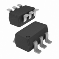
BF1214,115 NXP Semiconductors, BF1214,115 Datasheet - Page 13

BF1214,115
Manufacturer Part Number
BF1214,115
Description
MOSFET N-CH DUAL GATE 6V UMT6
Manufacturer
NXP Semiconductors
Datasheet
1.BF1214115.pdf
(18 pages)
Specifications of BF1214,115
Package / Case
SC-70-6, SC-88, SOT-363
Transistor Type
N-Channel Dual Gate
Frequency
400MHz
Gain
31dB
Voltage - Rated
6V
Current Rating
30mA
Noise Figure
0.9dB
Current - Test
18mA
Voltage - Test
5V
Configuration
Dual
Continuous Drain Current
30 mA
Drain-source Breakdown Voltage
6 V
Gate-source Breakdown Voltage
6 V
Maximum Operating Temperature
+ 150 C
Minimum Operating Temperature
- 65 C
Mounting Style
SMD/SMT
Transistor Polarity
N-Channel
Application
VHF/UHF
Channel Type
N
Channel Mode
Enhancement
Drain Source Voltage (max)
6V
Power Gain (typ)@vds
35@5VdB
Noise Figure (max)
1.8dB
Package Type
SOT-363
Pin Count
6
Input Capacitance (typ)@vds
2.2@5V@Gate 1/3.5@5V@Gate 2pF
Output Capacitance (typ)@vds
0.8@5VpF
Reverse Capacitance (typ)
0.02@5VpF
Operating Temp Range
-65C to 150C
Mounting
Surface Mount
Number Of Elements
2
Screening Level
Military
Lead Free Status / RoHS Status
Lead free / RoHS Compliant
Power - Output
-
Lead Free Status / Rohs Status
Lead free / RoHS Compliant
Other names
934061308115
BF1214 T/R
BF1214 T/R
BF1214 T/R
BF1214 T/R
Available stocks
Company
Part Number
Manufacturer
Quantity
Price
Part Number:
BF1214,115
Manufacturer:
NXP/恩智浦
Quantity:
20 000
NXP Semiconductors
BF1214_1
Product data sheet
Fig 20. Amplifier B: input admittance as a function of
Fig 22. Amplifier B: reverse transfer admittance and
b
(mS)
is
( S)
|y
, g
10
10
rs
10
10
10
10
|
10
is
1
1
2
1
2
3
2
V
I
frequency; typical values
V
I
phase as a function of frequency; typical values
10
D(B)
10
D(B)
DS(B)
DS(B)
= 18 mA.
= 18 mA.
= 5 V; V
= 5 V; V
G2-S
G2-S
= 4 V; V
= 4 V; V
10
10
2
2
|y
b
g
DS(A)
rs
rs
DS(A)
is
is
|
f (MHz)
f (MHz)
= 0 V;
= 0 V;
001aah011
001aah013
Rev. 01 — 30 October 2007
10
10
3
3
10
(deg)
10
10
1
3
rs
2
Fig 21. Amplifier B: forward transfer admittance and
Fig 23. Amplifier B: output admittance as a function of
b
os
(mS)
(mS)
|y
10
10
, g
fs
10
|
10
10
os
1
1
2
1
2
V
I
phase as a function of frequency; typical values
V
I
frequency; typical values
10
10
D(B)
D(B)
DS(B)
DS(B)
= 18 mA.
= 18 mA.
= 5 V; V
= 5 V; V
Dual N-channel dual gate MOSFET
G2-S
G2-S
= 4 V; V
= 4 V; V
10
10
2
2
|y
b
g
DS(A)
os
os
DS(A)
fs
fs
|
f (MHz)
f (MHz)
= 0 V;
= 0 V;
© NXP B.V. 2007. All rights reserved.
001aah012
001aah014
BF1214
10
10
3
3
10
(deg)
10
1
13 of 18
2
fs


