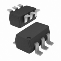
BF1214,115 NXP Semiconductors, BF1214,115 Datasheet - Page 2

BF1214,115
Manufacturer Part Number
BF1214,115
Description
MOSFET N-CH DUAL GATE 6V UMT6
Manufacturer
NXP Semiconductors
Datasheet
1.BF1214115.pdf
(18 pages)
Specifications of BF1214,115
Package / Case
SC-70-6, SC-88, SOT-363
Transistor Type
N-Channel Dual Gate
Frequency
400MHz
Gain
31dB
Voltage - Rated
6V
Current Rating
30mA
Noise Figure
0.9dB
Current - Test
18mA
Voltage - Test
5V
Configuration
Dual
Continuous Drain Current
30 mA
Drain-source Breakdown Voltage
6 V
Gate-source Breakdown Voltage
6 V
Maximum Operating Temperature
+ 150 C
Minimum Operating Temperature
- 65 C
Mounting Style
SMD/SMT
Transistor Polarity
N-Channel
Application
VHF/UHF
Channel Type
N
Channel Mode
Enhancement
Drain Source Voltage (max)
6V
Power Gain (typ)@vds
35@5VdB
Noise Figure (max)
1.8dB
Package Type
SOT-363
Pin Count
6
Input Capacitance (typ)@vds
2.2@5V@Gate 1/3.5@5V@Gate 2pF
Output Capacitance (typ)@vds
0.8@5VpF
Reverse Capacitance (typ)
0.02@5VpF
Operating Temp Range
-65C to 150C
Mounting
Surface Mount
Number Of Elements
2
Screening Level
Military
Lead Free Status / RoHS Status
Lead free / RoHS Compliant
Power - Output
-
Lead Free Status / Rohs Status
Lead free / RoHS Compliant
Other names
934061308115
BF1214 T/R
BF1214 T/R
BF1214 T/R
BF1214 T/R
Available stocks
Company
Part Number
Manufacturer
Quantity
Price
Part Number:
BF1214,115
Manufacturer:
NXP/恩智浦
Quantity:
20 000
NXP Semiconductors
2. Pinning information
3. Ordering information
BF1214_1
Product data sheet
1.4 Quick reference data
Table 1.
[1]
[2]
[3]
Table 2.
Table 3.
Symbol Parameter
V
I
P
C
C
NF
Xmod
T
Pin
1
2
3
4
5
6
Type number
BF1214
y
D
j
DS
tot
fs
iss(G1)
rss
T
Calculated from S-parameters.
Measured in
sp
is the temperature at the soldering point of the source lead.
drain-source voltage
drain current
total power dissipation
forward transfer admittance
input capacitance at gate1
reverse transfer capacitance f = 100 MHz
noise figure
cross modulation
junction temperature
Quick reference data for amplifier A and B
Discrete pinning
Ordering information
Description
drain (AMP A)
source
drain (AMP B)
gate1 (AMP B)
gate2
gate1 (AMP A)
Figure 24
Package
Name
-
Rev. 01 — 30 October 2007
test circuit.
Description
plastic surface-mounted package; 6 leads
Conditions
DC
DC
T
f = 100 MHz; T
I
f = 100 MHz
f = 400 MHz; Y
f = 800 MHz; Y
input level for k = 1 % at
40 dB AGC; f
f
D
unw
sp
= 18 mA
= 60 MHz
107 C
w
Simplified outline
j
S
S
= 50 MHz;
= 25 C;
= Y
= Y
Dual N-channel dual gate MOSFET
S(opt)
S(opt)
1
6
5
2
[3]
[1]
[2]
[2]
3
4
Min
-
-
-
27
-
-
-
-
102
-
Symbol
© NXP B.V. 2007. All rights reserved.
G1A
G1B
Typ
-
-
-
32
2.2
20
0.9
1.2
105
-
G2
BF1214
AMP A
AMP B
Max Unit
6
30
180
37
2.7
-
1.5
1.8
-
150
Version
SOT363
sym119
V
mA
mW
mS
pF
fF
dB
dB
dB V
2 of 18
C
DA
S
DB


