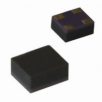
ATF-541M4-BLK Avago Technologies US Inc., ATF-541M4-BLK Datasheet - Page 14

ATF-541M4-BLK
Manufacturer Part Number
ATF-541M4-BLK
Description
IC ENHANCED MOD SUDIOMORPHIC HEM
Manufacturer
Avago Technologies US Inc.
Datasheet
1.ATF-541M4-BLK.pdf
(16 pages)
Specifications of ATF-541M4-BLK
Gain
17.5dB
Package / Case
4-MiniPak (1412)
Current Rating
120mA
Power - Output
21.4dBm
Frequency
2GHz
Transistor Type
pHEMT FET
Noise Figure
0.5dB
Current - Test
60mA
Voltage - Test
3V
Drain Source Voltage Vds
3V
Continuous Drain Current Id
120mA
Power Dissipation Pd
360mW
Noise Figure Typ
0.5dB
Rf Transistor Case
MiniPak
No. Of Pins
4
Frequency Max
10GHz
Drain Current Idss Max
60mA
Rohs Compliant
Yes
Lead Free Status / RoHS Status
Lead free / RoHS Compliant
Other names
Q2380948
14
0.043
Figure 3. PCB Pad Print for Minipak 1412.
Package (mm [inches ]).
ATF-541M4 Die Model
ATF-541M4 Minipak Model
This model can be used as a design tool. It has been tested on ADS for various specifications. However, for more precise
and accurate design, please refer to the measured data in this data sheet. For future improvements, Avago reserves
the right to change these models without prior notice.
SOURCE
1.1
Port
S1
Num=2
Port
G
Num=1
GATE
0.016
0.4
0.020
0.5
Advanced_Curtice2_Model
MESFETM1
NFET=yes
PFET=no
Vto=0.3
Beta=0.888
Lambda=72e-3
Alpha=13
Tau=
Tnom=16.85
Idstc=
Ucrit=-0.72
Vgexp=1.91
Gamds=1e-4
Vtotc=
Betatce=
Rgs=0.25 Ohm
0.016
0.4
INSIDE Package
Var
Egn
TLINP
TL3
Z=Z2 Ohm
L=23.6 mil
K=K
A=0.000
F=1 GHz
TanD=0.001
C
C1
C=0.28 pF
TLINP
TL9
Z=Z2 Ohm
L=11 mil
K=K
A=0.000
F=1 GHz
TanD=0.001
VAR
VAR1
K=5
Z2=85
Z1=30
0.012
0.3
0.020
0.5
L
L1
L=0.234 nH
R=0.001
L
L4
L=0.281 nH
R=0.001
0.012
0.3
TLINP
TL1
Z=Z2/2 Ohm
L=22 mil
K=K
A=0.000
F=1 GHz
TanD=0.001
Rf=
Gscap=2
Cgs=1.732 pF
Cgd=0.255 pF
Gdcap=2
Fc=0.65
Rgd=0.25 Ohm
Rd=1.0125 Ohm
Rg=1.7 Ohm
Rs=0.3375 Ohm
Ld=
Lg=0.188 nH
Ls=
Cds=0.273 pF
Rc=195 Ohm
GaAsFET
FET1
Mode1=MESFETM1
Mode=Nonlinear
This pad print provides allowance for
package placement by automated
assembly equipment without adding
excessive parasitics that could impair
the high frequency performance of
the ATF‑541M4. The layout is shown
with a footprint of the ATF‑541M4
superimposed on the PCB pads for
reference.
MSUB
MSub2
H=25.0 mil
Er=9.6
Mur=1
Cond=1.0E+50
Hu=3.9e+034 mil
T=0.15 mil
TanD=0
Rough=0 mil
MSub
Crf=0.1 F
Gsfwd=
Gsrev=
Gdfwd=
Gdrev=
R1=
R2=
Vbi=0.95
Vbr=
Vjr=
Is=
Ir=
Imax=
Xti=
Eg=
C=0.046 pF
L
L7
L=0.234 nH
R=0.001
TLINP
TL2
Z=Z2/2 Ohm
L=20 0 mil
K=K
A=0.000
F=1 GHz
TanD=0.001
L
L6
L=0.147 nH
R=0.001
C2
C
N=
Fnc=1 MHz
R=0.08
P=0.2
C=0.1
Taumdl=no
wVgfwd=
wBvgs=
wBvgd=
wBvds=
wldsmax=
wPmax=
AllParams=
TLINP
TL5
Z=Z2 Ohm
L=27.5 mil
K=K
A=0.000
F=1 GHz
TanD=0.001
TLINP
TL7
Z=Z2/2 Ohm
L=5.2 mil
K=K
A=0.000
F=1 GHz
TanD=0.001
For Further Information
The information presented here is an
introduction to the use of the ATF‑
541M4 enhancement mode PHEMT.
More detailed application circuit in‑
formation is available from Avago
Technologies. Consult the web page
or your local Avago Technologies sales
representative.
SOURCE
DRAIN
Port
S2
Num=4
Port
D
Num=3


