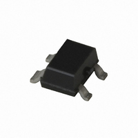
ATF-55143-TR1 Avago Technologies US Inc., ATF-55143-TR1 Datasheet - Page 2

ATF-55143-TR1
Manufacturer Part Number
ATF-55143-TR1
Description
IC TRANS E-PHEMT 2GHZ SOT-343
Manufacturer
Avago Technologies US Inc.
Datasheet
1.ATF-55143-TR1.pdf
(21 pages)
Specifications of ATF-55143-TR1
Transistor Type
pHEMT FET
Frequency
2GHz
Gain
17.7dB
Voltage - Rated
5V
Current Rating
100mA
Noise Figure
0.6dB
Current - Test
10mA
Voltage - Test
2.7V
Power - Output
14.4dBm
Package / Case
SC-70-4, SC-82-4, SOT-323-4, SOT-343
Lead Free Status / RoHS Status
Contains lead / RoHS non-compliant
Other names
516-1508-2
Available stocks
Company
Part Number
Manufacturer
Quantity
Price
Company:
Part Number:
ATF-55143-TR1
Manufacturer:
AVAGO
Quantity:
110 000
Company:
Part Number:
ATF-55143-TR1G
Manufacturer:
AVAGO
Quantity:
19 400
Company:
Part Number:
ATF-55143-TR1G
Manufacturer:
AVAGO
Quantity:
60 000
Part Number:
ATF-55143-TR1G
Manufacturer:
AVGO
Quantity:
20 000
2
ATF-55143 Absolute Maximum Ratings
I
I
P
P
T
T
Product Consistency Distribution Charts
Notes:
6. Distribution data sample size is 500 samples taken from 6 different wafers. Future wafers allocated to this product may have nominal values anywhere
7. Measurements made on production test board. This circuit represents a trade-off between an optimal noise match and a realizeable match based on
Symbol
V
V
V
θ
DS
GS
300
250
200
150
100
Figure 2. OIP3 @ 2.7 V, 10 mA.
LSL = 22.0, Nominal = 24.2
CH
STG
diss
in max.
jc
50
DS
GS
GD
0
between the upper and lower limits.
production test equipment. Circuit losses have been de-embedded from actual measurements.
Figure 1. Typical I-V Curves.
(V
22
GS
70
60
50
40
30
20
10
0
= 0.1 V per step)
0
-3 Std
23
1
OIP3 (dBm)
2
Parameter
Drain-Source Voltage
Gate-Source Voltage
Gate Drain Voltage
Drain Current
Gate Current
Total Power Dissipation
RF Input Power
Channel Temperature
Storage Temperature
Thermal Resistance
ESD (Human Body Model)
ESD (Machine Model)
24
V
3
DS
(V)
4
[5]
25
[2]
Cpk = 2.02
Stdev = 0.36
[5]
5
[2]
[4]
[2]
[2]
6
26
0.7V
0.6V
0.5V
0.4V
0.3V
[3]
7
[1]
[6, 7]
Figure 3. Gain @ 2.7 V, 10 mA.
USL = 18.5, LSL = 15.5, Nominal = 17.7
200
160
120
80
40
0
15
Units
V
V
V
mA
mA
mW
dBm
°C
°C
°C/W
V
V
Cpk = 1.023
Stdev = 0.28
16
GAIN (dB)
-3 Std
17
Absolute
Maximum
5
-5 to 1
-5 to 1
100
1
270
10
150
-65 to 150
235
200
25
18
+3 Std
19
Notes:
1. Operation of this device above any one of
2. Assumes DC quiescent conditions.
3. Source lead temperature is 25°C. Derate
4. Thermal resistance measured using
5. Device can safely handle +10 dBm RF Input
240
200
160
120
Figure 4. NF @ 2.7 V, 10 mA.
USL = 0.9, Nominal = 0.6
80
40
these parameters may cause permanent
damage.
4.3 mW/°C for T
150°C Liquid Crystal Measurement method.
Power as long as I
P
applications section for additional information.
0
0.43
1dB
drive level is bias circuit dependent. See
0.53
0.63
L
+3 Std
NF (dB)
> 87°C.
GS
is limited to 1 mA. I
0.73
Cpk = 3.64
Stdev = 0.031
0.83
0.93
GS
at


