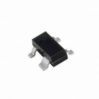
BFG505,215 NXP Semiconductors, BFG505,215 Datasheet - Page 2

BFG505,215
Manufacturer Part Number
BFG505,215
Description
TRANS NPN 6V 18MA SOT343N
Manufacturer
NXP Semiconductors
Datasheet
1.BFG505215.pdf
(13 pages)
Specifications of BFG505,215
Package / Case
SOT-143, SOT-143B, TO-253AA
Transistor Type
NPN
Voltage - Collector Emitter Breakdown (max)
15V
Frequency - Transition
9GHz
Noise Figure (db Typ @ F)
1.2dB ~ 2.1dB @ 900MHz
Power - Max
150mW
Dc Current Gain (hfe) (min) @ Ic, Vce
60 @ 5mA, 6V
Current - Collector (ic) (max)
18mA
Mounting Type
Surface Mount
Dc Collector/base Gain Hfe Min
60
Dc Current Gain Hfe Max
60 @ 5mA @ 6V
Mounting Style
SMD/SMT
Configuration
Dual
Transistor Polarity
NPN
Maximum Operating Frequency
9000 MHz (Typ)
Collector- Emitter Voltage Vceo Max
15 V
Emitter- Base Voltage Vebo
2.5 V
Continuous Collector Current
18 mA
Power Dissipation
150 mW
Maximum Operating Temperature
+ 175 C
Lead Free Status / RoHS Status
Lead free / RoHS Compliant
Gain
-
Lead Free Status / Rohs Status
Lead free / RoHS Compliant
Other names
934018760215
BFG505 T/R
BFG505 T/R
BFG505 T/R
BFG505 T/R
NXP Semiconductors
FEATURES
APPLICATIONS
RF front end applications in the GHz range, such as
analog and digital cellular telephones, cordless telephones
(CT1, CT2, DECT, etc.), radar detectors, pagers and
satellite TV tuners (SATV).
DESCRIPTION
NPN silicon planar epitaxial transistor in a 4-pin
dual-emitter SOT143B plastic package.
MARKING
QUICK REFERENCE DATA
BFG505
BFG505/X
V
V
I
P
h
C
f
G
F
TYPE NUMBER
C
T
S
FE
High power gain
Low noise figure
High transition frequency
Gold metallization ensures excellent reliability.
SYMBOL
CBO
CES
tot
re
NPN 9 GHz wideband transistors
UM
21
2
collector-base voltage
collector-emitter voltage R
collector current (DC)
total power dissipation
DC current gain
feedback capacitance
transition frequency
maximum unilateral
power gain
insertion power gain
noise figure
PARAMETER
CODE
%ME
%MK
open emitter
T
V
V
V
V
T
V
T
V
T
T
T
T
s
amb
amb
amb
s
amb
s
amb
s
amb
CE
CB
CE
CE
CE
CE
BE
=
=
=
= 6 V; I
= 6 V; I
= 6 V; I
= 6 V; I
= 6 V; I
= 6 V; I
= 0
130 C
= 25 C; f = 900 MHz
= 25 C; f = 2 GHz
= 25 C; f = 900 MHz
= 25 C; f = 900 MHz
= 25 C; f = 900 MHz
= 25 C; f = 2 GHz
opt
opt
opt
Rev. 04 - 22 November 2007
; V
; V
; V
CE
CE
CE
C
C
C
C
C
c
CONDITIONS
= 5 mA;
= 5 mA
= i
= 5 mA; f = 1 GHz
= 5 mA;
= 5 mA;
= 6 V; I
= 6 V; I
= 6 V; I
c
= 0; f = 1 MHz
PINNING
c
c
c
= 1.25 mA;
= 5 mA;
= 1.25 mA;
PIN
1
2
3
4
handbook, 2 columns
Fig.1 Simplified outline SOT143B.
collector
base
emitter
emitter
Top view
1
4
60
16
BFG505
MIN.
BFG505; BFG505/X
DESCRIPTION
0.2
9
20
13
17
1.2
1.6
1.9
120
TYP.
MSB014
Product specification
3
2
collector
emitter
base
emitter
20
15
18
150
250
1.7
2.1
MAX.
BFG505/X
2 of 13
V
V
mA
mW
pF
GHz
dB
dB
dB
dB
dB
dB
UNIT


