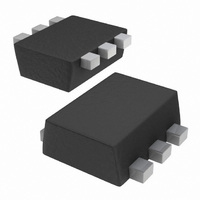
BCM857BV,115 NXP Semiconductors, BCM857BV,115 Datasheet - Page 11

BCM857BV,115
Manufacturer Part Number
BCM857BV,115
Description
TRANS PNP DBL 45V 100MA SOT-666
Manufacturer
NXP Semiconductors
Datasheet
1.BCM857BV315.pdf
(15 pages)
Specifications of BCM857BV,115
Package / Case
SS Mini-6 (SOT-666)
Transistor Type
2 PNP (Dual)
Current - Collector (ic) (max)
100mA
Voltage - Collector Emitter Breakdown (max)
45V
Vce Saturation (max) @ Ib, Ic
400mV @ 5mA, 100mA
Dc Current Gain (hfe) (min) @ Ic, Vce
200 @ 2mA, 5V
Power - Max
300mW
Frequency - Transition
175MHz
Mounting Type
Surface Mount
Dc Collector/base Gain Hfe Min
200
Gain Bandwidth Product Ft
175 MHz
Minimum Operating Temperature
- 65 C
Configuration
Dual
Transistor Polarity
PNP
Mounting Style
SMD/SMT
Collector- Emitter Voltage Vceo Max
- 45 V
Emitter- Base Voltage Vebo
- 5 V
Continuous Collector Current
- 100 mA
Maximum Dc Collector Current
- 200 mA
Power Dissipation
200 mW
Maximum Operating Frequency
175 MHz
Maximum Operating Temperature
+ 150 C
Lead Free Status / RoHS Status
Lead free / RoHS Compliant
Current - Collector Cutoff (max)
-
Lead Free Status / Rohs Status
Lead free / RoHS Compliant
Other names
934059435115
NXP Semiconductors
BCM857BV_BS_DS_6
Product data sheet
Fig 16. Wave soldering footprint SOT363 (SC-88)
Fig 17. Reflow soldering footprint SOT457 (SC-74)
4.5
3.30
Dimensions in mm
2.825
1.3
0.95
Rev. 06 — 28 August 2009
2.45
5.3
1.3
3.45
1.95
1.60
1.70
3.10
3.20
1.5
1.5
msc422
0.3
0.45 0.55
PNP/PNP matched double transistors
BCM857BV/BS/DS
2.5
direction during soldering
Dimensions in mm
© NXP B.V. 2009. All rights reserved.
solder lands
preferred transport
solder resist
occupied area
solder paste
solder lands
solder resist
occupied area
sot363_fw
11 of 15


