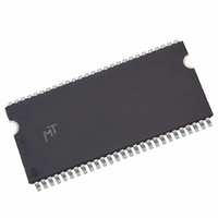
MT48LC4M16A2P-75:G TR Micron Technology Inc, MT48LC4M16A2P-75:G TR Datasheet - Page 23

MT48LC4M16A2P-75:G TR
Manufacturer Part Number
MT48LC4M16A2P-75:G TR
Description
DRAM Chip SDRAM 64M-Bit 4Mx16 3.3V 54-Pin TSOP-II T/R
Manufacturer
Micron Technology Inc
Type
SDRAMr
Datasheet
1.MT48LC4M16A2P-75G_TR.pdf
(72 pages)
Specifications of MT48LC4M16A2P-75:G TR
Density
64 Mb
Maximum Clock Rate
133 MHz
Package
54TSOP-II
Address Bus Width
14 Bit
Operating Supply Voltage
3.3 V
Maximum Random Access Time
6|5.4 ns
Operating Temperature
0 to 70 °C
Format - Memory
RAM
Memory Type
SDRAM
Memory Size
64M (4M x 16)
Speed
133MHz
Interface
Parallel
Voltage - Supply
3 V ~ 3.6 V
Package / Case
54-TSOP II
Organization
4Mx16
Address Bus
14b
Access Time (max)
6/5.4ns
Operating Supply Voltage (typ)
3.3V
Package Type
TSOP-II
Operating Temp Range
0C to 70C
Operating Supply Voltage (max)
3.6V
Operating Supply Voltage (min)
3V
Supply Current
140mA
Pin Count
54
Mounting
Surface Mount
Operating Temperature Classification
Commercial
Lead Free Status / RoHS Status
Lead free / RoHS Compliant
Other names
557-1088-2
Figure 10:
PDF: 09005aef80725c0b/Source: 09005aef806fc13c
64MSDRAM_2.fm - Rev. N 12/08 EN
READ Command
Data from any READ burst may be truncated with a subsequent READ command, and
data from a fixed-length READ burst may be immediately followed by data from a READ
command. In either case, a continuous flow of data can be maintained. The first data
element from the new burst follows either the last element of a completed burst or the
last desired data element of a longer burst which is being truncated.
The new READ command should be issued x cycles before the clock edge at which the
last desired data element is valid, where x = CL -1. This is shown in Figure 12 on page 25
for CL = 2 and CL = 3; data element n + 3 is either the last of a burst of four or the last
desired of a longer burst. The 64Mb SDRAM uses a pipelined architecture and therefore
does not require the 2n rule associated with a prefetch architecture. A READ command
can be initiated on any clock cycle following a previous READ command. Full-speed
random read accesses can be performed to the same bank, as shown in Figure 13 on
page 26, or each subsequent READ may be performed to a different bank.
A8, A9, A11: x16
A9, A11: x8
A0–A9: x4
A0–A8: x8
A0–A7: x16
BA0, BA1
A11: x4
RAS#
CAS#
CLK
CKE
WE#
CS#
A10
HIGH
DISABLE AUTO PRECHARGE
ENABLE AUTO PRECHARGE
COLUMN
ADDRESS
ADDRESS
23
BANK
DON’T CARE
Micron Technology, Inc., reserves the right to change products or specifications without notice.
64Mb: x4, x8, x16 SDRAM
©2000 Micron Technology, Inc. All rights reserved.
Commands


