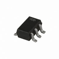
PUMB30,115 NXP Semiconductors, PUMB30,115 Datasheet - Page 7

PUMB30,115
Manufacturer Part Number
PUMB30,115
Description
TRANS PNP/PNP W/RES 50V SOT-363
Manufacturer
NXP Semiconductors
Datasheet
1.PUMB30115.pdf
(10 pages)
Specifications of PUMB30,115
Package / Case
SC-70-6, SC-88, SOT-363
Transistor Type
2 PNP - Pre-Biased (Dual)
Current - Collector (ic) (max)
100mA
Voltage - Collector Emitter Breakdown (max)
50V
Resistor - Base (r1) (ohms)
2.2K
Dc Current Gain (hfe) (min) @ Ic, Vce
30 @ 20mA, 5V
Vce Saturation (max) @ Ib, Ic
150mV @ 500µA, 10mA
Current - Collector Cutoff (max)
1µA
Power - Max
300mW
Mounting Type
Surface Mount
Configuration
Dual
Transistor Polarity
PNP
Typical Input Resistor
2.2 KOhm
Mounting Style
SMD/SMT
Collector- Emitter Voltage Vceo Max
50 V
Peak Dc Collector Current
100 mA
Maximum Operating Temperature
+ 150 C
Minimum Operating Temperature
- 65 C
Lead Free Status / RoHS Status
Lead free / RoHS Compliant
Frequency - Transition
-
Resistor - Emitter Base (r2) (ohms)
-
Lead Free Status / RoHS Status
Lead free / RoHS Compliant, Lead free / RoHS Compliant
Other names
934059933115
PUMB30 T/R
PUMB30 T/R
PUMB30 T/R
PUMB30 T/R
NXP Semiconductors
PEMB30_PUMB30_2
Product data sheet
Fig 7.
2
1.7
1.075
Reflow soldering is the only recommended soldering method.
Reflow soldering footprint SOT666
0.538
PNP/PNP double resistor-equipped transistors; R1 = 2.2 k , R2 = open
0.55
(2 )
Rev. 02 — 2 September 2009
0.45
(4 )
(4 )
0.5
2.75
2.45
2.1
1.6
1.7
0.65
(2 )
(2 )
0.6
PEMB30; PUMB30
(6 )
0.4
0.325
0.25
(2 )
(4 )
0.375
(2 )
(4 )
0.3
Dimensions in mm
© NXP B.V. 2009. All rights reserved.
solder lands
placement area
solder paste
occupied area
sot666_fr
7 of 10


