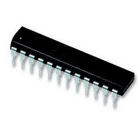
SCC2691AC1N24 NXP Semiconductors, SCC2691AC1N24 Datasheet - Page 16

SCC2691AC1N24
Manufacturer Part Number
SCC2691AC1N24
Description
UART 1-CH 5V 24-Pin PDIP Tube
Manufacturer
NXP Semiconductors
Datasheet
1.SCC2691AC1N24.pdf
(25 pages)
Specifications of SCC2691AC1N24
Package
24PDIP
Number Of Channels Per Chip
1
Maximum Data Rate
0.1152 MBd
Transmitter And Receiver Fifo Counter
No
Operating Supply Voltage
5 V
Minimum Single Supply Voltage
4.5 V
Maximum Processing Temperature
260 °C
Maximum Supply Current
2 mA
No. Of Channels
1
Supply Voltage Range
4.5V To 5.5V
Operating Temperature Range
0°C To +70°C
Digital Ic Case Style
DIP
No. Of Pins
24
Uart Type
Asynchronous
Termination Type
DIP
Uart Features
False-Start Bit Detection, Line Break Detection And Generation
Rohs Compliant
Yes
Lead Free Status / RoHS Status
Lead free / RoHS Compliant
Available stocks
Company
Part Number
Manufacturer
Quantity
Price
Company:
Part Number:
SCC2691AC1N24
Manufacturer:
NXP
Quantity:
19 281
Part Number:
SCC2691AC1N24
Manufacturer:
XNP/恩智浦
Quantity:
20 000
Philips Semiconductors
2006 Aug 04
C/T CLK
Universal asynchronous receiver/transmitter (UART)
X1/CLK
RxC
TxC
NOTES:
1. INTRN or MPO when used as interrupt outputs.
2. The test for open drain outputs is intended to guarantee switching of the output transistor. Measurement of this response is referenced from the midpoint of the switching signal,
V
are pronounced and can greatly affect the resultant measurement.
MPO
WRN
RDN
M
MPI
, to a point 0.5V above V
FROM EXTERNAL
CLK
DRIVING
SOURCE
t
PS
INTERRUPT
INTERRUPT
5V
OUTPUT
OUTPUT
OL
. This point represents noise margin that assures true switching has occurred. Beyond this level, the effects of external circuitry and test environment
t
t
470
t
t
WRN
CLK
CTC
N/C
RDN
Rx
Tx
1
1
t
PH
X1
X2
t
t
t
t
CLK
CTC
Rx
Tx
Figure 6. Interrupt Timing
Figure 7. Clock Timing
Figure 5. I/O Timing
t
IR
16
TYPE OF OPERATION . . . . . .PARALLEL RESONANT, FUND. MODE
FREQUENCY. . . . . . . . . . . . . . 2–4MHz
LOAD CAPACITANCE (C
V
M
t
IR
TYPICAL CRYSTAL SPECIFICATION
C1
C2
V
L
Y1 = 3.6864MHz, C
). . . 20 or 32pF (typical)
t
C1 = C2 = 24pF
OL
PD
V
OL
+0.5V
+0.5V
V
Y1
OL
V
OL
L
= 20pF
X1/CLK
X2
50k
to
150k
SCC2691
SD00125
SCC2691
Product data sheet
SD00127
SD00126


