CY2314ANZSC-1 Cypress Semiconductor Corp, CY2314ANZSC-1 Datasheet - Page 2
CY2314ANZSC-1
Manufacturer Part Number
CY2314ANZSC-1
Description
Manufacturer
Cypress Semiconductor Corp
Datasheet
1.CY2314ANZSC-1.pdf
(8 pages)
Specifications of CY2314ANZSC-1
Number Of Outputs
14
Operating Supply Voltage (max)
3.465V
Operating Temp Range
0C to 70C
Propagation Delay Time
30ns
Operating Supply Voltage (min)
3.135V
Mounting
Surface Mount
Pin Count
28
Operating Supply Voltage (typ)
3.3V
Package Type
SOIC
Duty Cycle
55%
Operating Temperature Classification
Commercial
Lead Free Status / RoHS Status
Not Compliant
Available stocks
Company
Part Number
Manufacturer
Quantity
Price
Company:

Part Number:
CY2314ANZSC-1
Manufacturer:
HARRIS
Quantity:
221
Part Number:
CY2314ANZSC-1
Manufacturer:
CYPRESS/赛普拉斯
Quantity:
20 000


Pin Configuration
Device Functionality
Serial Configuration Map
■
■
■
Table 1. Byte 0: SDRAM Active/Inactive Register
(1 = Enable, 0 = Disable), Default = Enabled
Document #: 38-07143 Rev. *B
Bit 7 11
Bit 6 10
Bit 5 --
Bit 4 --
Bit 3 7
Bit 2 6
Bit 1 3
Bit 0 2
Bit
The serial bits are read by the clock driver in the following order:
Reserved and unused bits should be programmed to “0”
Serial interface address for the CY2314ANZ is:
A6
1
Byte 0 - Bits 7, 6, 5, 4, 3, 2, 1, 0
Byte 1 - Bits 7, 6, 5, 4, 3, 2, 1, 0
Byte N - Bits 7, 6, 5, 4, 3, 2, 1, 0
Pin #
A5
1
OE
0
1
SDRAM5 (Active/Inactive)
SDRAM4 (Active/Inactive)
Reserved, Drive to 0
Reserved, Drive to 0
SDRAM3 (Active/Inactive)
SDRAM2 (Active/Inactive)
SDRAM1 (Active/Inactive)
SDRAM0 (Active/Inactive)
A4
0
A3
1
Description
A2
0
SDRAM [0-13]
1 x BUF_IN
A1
0
High-Z
SDRAM12
SDRAM0
SDRAM1
SDRAM2
SDRAM3
SDRAM4
SDRAM5
A0
BUF_IN
1
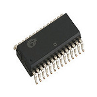
Figure 1. 28-Pin SOIC Top View
SDATA
V
DDIIC
V
V
V
V
DD
DD
SS
SS
R/W
----
1
2
3
4
5
6
7
8
9
10
11
12
13
14
Table 2. Byte 1: SDRAM Active/Inactive Register
(1 = Active, 0 = Inactive), Default = Active
Table 3. Byte 2: SDRAM Active/Inactive Register
(1 = Active, 0 = Inactive), Default = Active
28
27
26
25
24
23
22
21
20
19
18
17
16
15
Bit 7
Bit 6
Bit 5
Bit 4
Bit 3
Bit 2
Bit 1
Bit 0
Bit 7
Bit 6
Bit 5
Bit 4
Bit 3
Bit 2
Bit 1
Bit 0
Bit
Bit
V
V
V
V
OE
V
SCLK
SDRAM11
SDRAM10
SDRAM9
SDRAM8
SDRAM7
SDRAM6
SDRAM13
DD
SS
DD
SS
SSIIC
27
26
23
22
--
--
19
18
17
12
--
--
--
--
--
--
Pin #
Pin #
SDRAM13 (Active/Inactive)
SDRAM12 (Active/Inactive)
Reserved, Drive to 0
Reserved, Drive to 0
Reserved, Drive to 0
Reserved, Drive to 0
Reserved, Drive to 0
Reserved, Drive to 0
SDRAM11 (Active/Inactive)
SDRAM10 (Active/Inactive)
SDRAM9 (Active/Inactive)
SDRAM8 (Active/Inactive)
Reserved, Drive to 0
Reserved, Drive to 0
SDRAM7 (Active/Inactive)
SDRAM6 (Active/Inactive)
Description
Description
CY2314ANZ
Page 2 of 8
[+] Feedback
Related parts for CY2314ANZSC-1
Image
Part Number
Description
Manufacturer
Datasheet
Request
R

Part Number:
Description:
Manufacturer:
Cypress Semiconductor Corp
Datasheet:
Part Number:
Description:
Manufacturer:
Cypress Semiconductor Corp
Datasheet:
Part Number:
Description:
Manufacturer:
Cypress Semiconductor Corp
Datasheet:
Part Number:
Description:
Manufacturer:
Cypress Semiconductor Corp
Datasheet:
Part Number:
Description:
Manufacturer:
Cypress Semiconductor Corp
Datasheet: