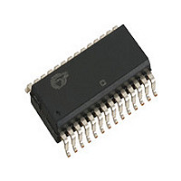
CY2314ANZSC-1 Cypress Semiconductor Corp, CY2314ANZSC-1 Datasheet - Page 4

CY2314ANZSC-1
Manufacturer Part Number
CY2314ANZSC-1
Description
Manufacturer
Cypress Semiconductor Corp
Datasheet
1.CY2314ANZSC-1.pdf
(8 pages)
Specifications of CY2314ANZSC-1
Number Of Outputs
14
Operating Supply Voltage (max)
3.465V
Operating Temp Range
0C to 70C
Propagation Delay Time
30ns
Operating Supply Voltage (min)
3.135V
Mounting
Surface Mount
Pin Count
28
Operating Supply Voltage (typ)
3.3V
Package Type
SOIC
Duty Cycle
55%
Operating Temperature Classification
Commercial
Lead Free Status / RoHS Status
Not Compliant
Available stocks
Company
Part Number
Manufacturer
Quantity
Price
Company:
Part Number:
CY2314ANZSC-1
Manufacturer:
HARRIS
Quantity:
221
Part Number:
CY2314ANZSC-1
Manufacturer:
CYPRESS/赛普拉斯
Quantity:
20 000
Switching Characteristics
Switching Waveforms
Document #: 38-07143 Rev. *B
Notes
t
t
t
t
t
t
t
4. All parameters specified with loaded outputs.
5. Duty cycle of input clock is 50%. Rising and falling edge rate of the input clock is greater than 1 V/ns.
Parameter
3
4
5
6
7
8
9
Maximum Operating Frequency
Duty Cycle
Rising Edge Rate
Falling Edge Rate
Output to Output Skew
SDRAM Buffer LH Propogation
Delay
SDRAM Buffer HL Propogation
Delay
SDRAM Buffer Enable Delay
SDRAM Buffer Disable Delay
[3]
[3]
[3, 5]
Name
= t
OUTPUT
[3]
[3]
2
OUTPUT
OUTPUT
÷ t
1
[4]
[3]
Over the Operating Range
t
0.4V
3
[3]
1.5V
[3]
Figure 3. All Outputs Rise/Fall Time
2.4V
Figure 4. Output-Output Skew
1.5V
Figure 2. Duty Cycle Timing
t
5
Measured at 1.5V
Measured between 0.4V and 2.4V
Measured between 2.4V and 0.4V
All outputs equally loaded
Input edge greater than 1 V/ns
Input edge greater than 1 V/ns
Input edge greater than 1 V/ns
Input edge greater than 1 V/ns
t
2
1.5V
Test Conditions
1.5V
t
1
2.4V
0.4V
t
4
1.5V
–250
45.0
Min
0.9
0.9
1.0
1.0
1.0
1.0
3.3V
0V
50.0
Typ
1.5
1.5
3.5
3.5
20
5
+250
Max
55.0
CY2314ANZ
100
4.0
4.0
5.0
5.0
12
30
MHz
Page 4 of 8
Unit
V/ns
V/ns
ns
ns
ns
ns
ps
%
[+] Feedback


