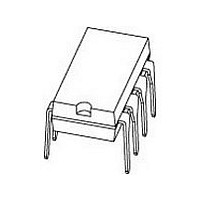
PCF8583P NXP Semiconductors, PCF8583P Datasheet - Page 22

PCF8583P
Manufacturer Part Number
PCF8583P
Description
Manufacturer
NXP Semiconductors
Datasheet
1.PCF8583P.pdf
(37 pages)
Specifications of PCF8583P
Bus Type
Serial (2-Wire, I2C)
Operating Supply Voltage (typ)
3.3/5V
Package Type
PDIP
Operating Supply Voltage (max)
6V
Operating Supply Voltage (min)
2.5V
Operating Temperature Classification
Industrial
Operating Temperature (max)
85C
Operating Temperature (min)
-40C
Pin Count
8
Mounting
Through Hole
Date Format
DW:DM:M:Y
Time Format
HH:MM:SS:hh
Lead Free Status / RoHS Status
Compliant
Available stocks
Company
Part Number
Manufacturer
Quantity
Price
Company:
Part Number:
PCF8583P
Manufacturer:
SAMSUNG
Quantity:
1 001
Company:
Part Number:
PCF8583P
Manufacturer:
NXPLIPS
Quantity:
5 510
Part Number:
PCF8583P
Manufacturer:
PHILIPS/飞利浦
Quantity:
20 000
Company:
Part Number:
PCF8583P/F5
Manufacturer:
TI
Quantity:
90
Company:
Part Number:
PCF8583P/F5,112
Manufacturer:
LTC
Quantity:
147
Part Number:
PCF8583PN
Manufacturer:
PHI
Quantity:
20 000
NXP Semiconductors
Table 8.
V
[1]
[2]
PCF8583
Product data sheet
Symbol
Oscillator
C
Δf
f
Quartz crystal parameters (f = 32.768 kHz)
R
C
C
I
f
t
t
t
t
t
t
t
t
t
t
t
t
clk(ext)
2
SCL
SP
BUF
SU;STA
HD;STA
LOW
HIGH
r
f
SU;DAT
HD;DAT
VD;DAT
SU;STO
DD
C-bus timing (see
OSCO
S
L
trim
osc
= 2.5 V to 6.0 V; V
Event counter mode only.
All timing values are valid within the operating supply voltage, ambient temperature range, reference to V
voltage swing of V
/f
osc
Dynamic characteristics
Parameter
capacitance on pin OSCO
relative oscillator frequency
variation
external clock frequency
series resistance
parallel load capacitance
trimmer capacitance
SCL clock frequency
pulse width of spikes that
must be suppressed by the
input filter
bus free time between a
STOP and START condition
set-up time for a repeated
START condition
hold time (repeated) START
condition
LOW period of the SCL clock
HIGH period of the SCL clock
rise time of both SDA and
SCL signals
fall time of both SDA and SCL
signals
data set-up time
data hold time
data valid time
set-up time for STOP
condition
10.2 Dynamic characteristics
SS
Figure
SS
to V
= 0 V; T
DD
21)
.
[2]
amb
=
−
40
All information provided in this document is subject to legal disclaimers.
°
C to +85
Conditions
for ΔV
V
on pin OSCI
DD
Rev. 06 — 6 October 2010
= 1.5 V
DD
°
C unless otherwise specified.
= 100 mV; T
amb
= 25 °C;
Clock and calendar with 240 x 8-bit RAM
[1]
Min
-
-
-
-
-
5
-
-
4.7
4.7
4.0
4.7
4.0
-
-
250
0
-
4.0
Typ
40
0.2
-
-
10
-
-
-
-
-
-
-
-
-
-
-
-
-
-
IL
and V
PCF8583
© NXP B.V. 2010. All rights reserved.
IH
Max
-
-
1
40
-
25
100
100
-
-
-
-
-
1.0
0.3
-
-
3.4
-
and with an input
Unit
pF
ppm
MHz
kΩ
pF
pF
kHz
ns
μs
μs
μs
μs
μs
μs
μs
ns
ns
μs
μs
22 of 37


