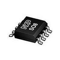
PCF8593T NXP Semiconductors, PCF8593T Datasheet - Page 15

PCF8593T
Manufacturer Part Number
PCF8593T
Description
Manufacturer
NXP Semiconductors
Datasheet
1.PCF8593T.pdf
(35 pages)
Specifications of PCF8593T
Bus Type
Serial (I2C)
User Ram
8Byte
Package Type
SO
Operating Supply Voltage (max)
6V
Operating Temperature Classification
Industrial
Operating Temperature (max)
85C
Operating Temperature (min)
-40C
Pin Count
8
Mounting
Surface Mount
Date Format
DW:DM:M:Y
Time Format
HH:MM:SS:hh
Lead Free Status / RoHS Status
Compliant
Available stocks
Company
Part Number
Manufacturer
Quantity
Price
Company:
Part Number:
PCF8593T
Manufacturer:
NXP
Quantity:
5 510
Part Number:
PCF8593T
Manufacturer:
PHILIPS/飞利浦
Quantity:
20 000
Part Number:
PCF8593T-1
Manufacturer:
PHILIPS/飞利浦
Quantity:
20 000
Part Number:
PCF8593T/1
Manufacturer:
NXP/恩智浦
Quantity:
20 000
Part Number:
PCF8593T/1,112
Manufacturer:
NXP/恩智浦
Quantity:
20 000
Company:
Part Number:
PCF8593T/1,118
Manufacturer:
LT
Quantity:
232
Part Number:
PCF8593T/1118
Manufacturer:
NXP/恩智浦
Quantity:
20 000
NXP Semiconductors
PCF8593
Product data sheet
Fig 16. System configuration
SCL
SDA
8.1.4 Acknowledge
TRANSMITTER
RECEIVER
MASTER
The number of data bytes transferred between the START and STOP conditions from
transmitter to receiver is unlimited. Each byte of eight bits is followed by an acknowledge
cycle.
Acknowledgement on the I
Fig 17. Acknowledgement on the I
•
•
•
•
A slave receiver, which is addressed, must generate an acknowledge after the
reception of each byte.
Also a master receiver must generate an acknowledge after the reception of each
byte that has been clocked out of the slave transmitter.
The device that acknowledges must pull-down the SDA line during the acknowledge
clock pulse, so that the SDA line is stable LOW during the HIGH period of the
acknowledge related clock pulse (set-up and hold times must be taken into
consideration).
A master receiver must signal an end of data to the transmitter by not generating an
acknowledge on the last byte that has been clocked out of the slave. In this event, the
transmitter must leave the data line HIGH to enable the master to generate a STOP
condition.
by transmitter
data output
by receiver
data output
SCL from
master
RECEIVER
SLAVE
All information provided in this document is subject to legal disclaimers.
condition
START
Rev. 04 — 6 October 2010
S
2
C-bus is illustrated in
TRANSMITTER
RECEIVER
SLAVE
1
2
C-bus
2
TRANSMITTER
Figure
MASTER
17.
Low power clock and calendar
not acknowledge
acknowledge
8
TRANSMITTER
RECEIVER
MASTER
acknowledgement
clock pulse for
PCF8593
© NXP B.V. 2010. All rights reserved.
mba605
9
mbc602
15 of 35


